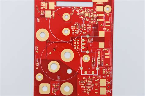
Introduction to Heavy Copper PCB
Heavy copper PCBs are printed circuit boards that feature thicker copper traces than standard PCBs. These boards are designed to handle higher currents and temperatures, making them ideal for power electronics, automotive applications, and other high-performance systems. In this comprehensive guide, we’ll dive into the world of heavy copper PCB manufacturing, exploring the benefits, applications, design considerations, and manufacturing processes involved.
What is a Heavy Copper PCB?
A heavy copper PCB is a printed circuit board with copper traces that are thicker than the standard 1 oz. (35 µm) copper used in most PCBs. The thickness of the copper can range from 2 oz. (70 µm) to 20 oz. (700 µm) or more, depending on the application requirements. The increased copper thickness allows for higher current carrying capacity and improved thermal management.
Benefits of Heavy Copper PCBs
- Higher current carrying capacity
- Improved thermal management
- Enhanced mechanical strength
- Reduced voltage drop
- Better signal integrity
Applications of Heavy Copper PCB
Heavy copper PCBs find applications in various industries where high current handling and thermal management are critical. Some of the key applications include:
Power Electronics
- Power supplies
- Inverters
- Motor drives
- Uninterruptible power supplies (UPS)
Automotive Electronics
- Electric vehicle battery management systems
- Engine control units (ECUs)
- Charging systems
- High-power lighting systems
Industrial Equipment
- Welding machines
- Induction heating systems
- High-power lasers
- Industrial automation systems
Telecommunications
- Base station power amplifiers
- Satellite communication systems
- High-power RF transmitters

Designing Heavy Copper PCBs
Designing heavy copper PCBs requires careful consideration of various factors to ensure optimal performance and manufacturability. Some of the key design considerations include:
Copper Thickness Selection
The copper thickness should be selected based on the current carrying requirements and thermal management needs of the application. The following table provides a general guideline for selecting copper thickness based on current requirements:
| Copper Thickness (oz.) | Current Carrying Capacity (A/mm) |
|---|---|
| 1 | 0.5 |
| 2 | 1.0 |
| 3 | 1.5 |
| 4 | 2.0 |
| 6 | 3.0 |
| 8 | 4.0 |
| 10 | 5.0 |
Trace Width and Spacing
The trace width and spacing should be designed to accommodate the increased copper thickness while maintaining acceptable manufacturability. Wider traces and increased spacing may be necessary to ensure proper etching and to avoid short circuits.
Thermal Management
Heavy copper PCBs generate more heat than standard PCBs due to the higher current carrying capacity. Proper thermal management techniques should be employed, such as the use of thermal vias, heat sinks, and appropriate component placement to ensure efficient heat dissipation.
Layer Stack-up
The layer stack-up should be designed to optimize signal integrity and power distribution. The heavy copper layers should be strategically placed to minimize voltage drop and ensure proper current flow. Ground planes and power planes should be incorporated to provide low-impedance paths for return currents and to minimize electromagnetic interference (EMI).

Manufacturing Heavy Copper PCBs
The manufacturing process for heavy copper PCBs differs from that of standard PCBs due to the increased copper thickness. Some of the key manufacturing considerations include:
Copper Deposition
The heavy copper layers are typically deposited using electroplating or a combination of electroplating and foil lamination. The copper deposition process must be carefully controlled to ensure uniform thickness and adherence to the substrate.
Etching
Etching heavy copper PCBs requires longer etch times and more precise control of the etching process parameters. The etchant chemistry and concentration, as well as the etching temperature and agitation, must be optimized to achieve the desired trace geometry and to minimize undercut.
Drilling and Plating
Drilling and plating heavy copper PCBs can be challenging due to the increased thickness of the copper layers. High-speed drilling and specialized drill bits may be necessary to ensure clean and accurate hole formation. The plating process must also be optimized to ensure proper coverage and adhesion of the plated copper in the holes.
Inspection and Testing
Heavy copper PCBs require thorough inspection and testing to ensure they meet the specified performance and quality requirements. Visual inspection, electrical testing, and thermal imaging are commonly used techniques to verify the integrity of the PCB and to identify any potential issues.

Frequently Asked Questions (FAQ)
1. What is the maximum copper thickness that can be used in heavy copper PCBs?
The maximum copper thickness that can be used in heavy copper PCBs depends on the manufacturing capabilities of the PCB fabricator. Typically, copper thicknesses up to 20 oz. (700 µm) are achievable, but some specialized manufacturers may be able to produce even thicker copper layers.
2. How does the use of heavy copper affect the cost of PCB manufacturing?
The use of heavy copper in PCBs increases the manufacturing cost due to the additional copper material, longer processing times, and specialized equipment required. The cost increase is proportional to the copper thickness and the complexity of the PCB design.
3. Can heavy copper PCBs be combined with other PCB technologies, such as high-frequency materials or flexible substrates?
Yes, heavy copper PCBs can be combined with other PCB technologies to meet specific application requirements. For example, heavy copper layers can be incorporated into high-frequency PCBs using low-loss dielectric materials, or they can be combined with flexible substrates to create flexible heavy copper PCBs.
4. Are there any special considerations for soldering components on heavy copper PCBs?
Soldering components on heavy copper PCBs may require higher soldering temperatures and longer dwell times to ensure proper solder joint formation. The increased thermal mass of the heavy copper layers can affect the heat transfer during the soldering process, so appropriate soldering techniques and parameters should be used.
5. How can I select the right PCB manufacturer for my heavy copper PCB project?
When selecting a PCB manufacturer for your heavy copper PCB project, consider factors such as their experience with heavy copper PCBs, manufacturing capabilities, quality control processes, and customer support. Look for manufacturers who specialize in heavy copper PCBs and have a proven track record of delivering high-quality boards. Request samples and references to evaluate their capabilities and quality before placing an order.
Conclusion
Heavy copper PCBs offer numerous benefits for applications that require high current carrying capacity and improved thermal management. By understanding the design considerations, manufacturing processes, and application requirements, engineers can effectively leverage heavy copper PCBs to enhance the performance and reliability of their products.
When designing and manufacturing heavy copper PCBs, it is essential to work closely with experienced PCB manufacturers who have the expertise and capabilities to handle the unique challenges associated with heavy copper. By selecting the right partner and following best practices in design and manufacturing, you can unlock the full potential of heavy copper PCBs and create innovative solutions for your high-performance applications.
No responses yet