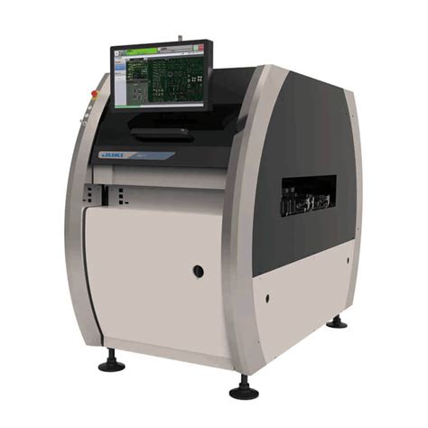
What is AOI Inspection?
AOI (Automated Optical Inspection) is a vital process in the manufacturing of printed circuit boards (PCBs) and other electronic components. It uses advanced camera systems and image processing software to detect defects, missing components, or incorrect placements on PCBs, ensuring the quality and reliability of the final product.
How AOI Inspection Works
- The PCB is placed under a high-resolution camera system.
- The camera captures images of the PCB from various angles and lighting conditions.
- The captured images are processed by sophisticated software, which compares them to a pre-defined set of design specifications.
- Any discrepancies or defects are flagged for further review or correction.
Benefits of AOI Inspection
1. Improved Quality Control
AOI inspection ensures that every PCB meets the required quality standards, reducing the risk of defective products reaching the end-user.
2. Increased Efficiency
Automated inspection is much faster than manual inspection, allowing for higher production throughput and reduced labor costs.
3. Early Defect Detection
By catching defects early in the manufacturing process, AOI inspection minimizes the cost and time associated with reworking or scrapping defective boards.
Types of AOI Inspection Systems
1. 2D AOI Systems
These systems use standard 2D cameras to capture images of the PCB surface. They are suitable for inspecting solder joints, component placement, and other surface-level features.
2. 3D AOI Systems
3D AOI systems use advanced techniques like structured light or laser scanning to create a 3D model of the PCB. This allows for the inspection of component height, coplanarity, and other three-dimensional aspects.
| Feature | 2D AOI | 3D AOI |
|---|---|---|
| Surface-level inspection | Yes | Yes |
| 3D inspection | No | Yes |
| Cost | Lower | Higher |
| Complexity | Lower | Higher |

Implementing AOI Inspection
1. Choose the Right System
Consider factors such as the complexity of your PCBs, required inspection speed, and budget when selecting an AOI system.
2. Develop Inspection Programs
Create inspection programs that define the design specifications and acceptance criteria for your PCBs.
3. Integrate with Manufacturing Process
Integrate the AOI system into your manufacturing process, ensuring smooth handoff between the inspection and subsequent stages.
4. Train Personnel
Provide adequate training to your personnel on operating and maintaining the AOI system.
Frequently Asked Questions (FAQ)
1. How accurate is AOI inspection?
Modern AOI systems can achieve very high accuracy, often detecting defects as small as 0.02 mm. However, the actual accuracy depends on factors like the complexity of the PCB, the quality of the inspection program, and the capabilities of the specific AOI system.
2. Can AOI inspection replace manual inspection?
While AOI inspection can significantly reduce the need for manual inspection, it is often used in conjunction with manual inspection for critical components or to verify automated inspection results.
3. What types of defects can AOI inspection detect?
AOI inspection can detect a wide range of defects, including:
– Missing, misaligned, or incorrect components
– Solder joint defects (bridges, voids, insufficient solder, etc.)
– PCB surface defects (scratches, contamination, etc.)
– Component polarity and orientation issues
4. How fast is AOI inspection?
AOI inspection speed varies depending on the system and the complexity of the PCB. High-end systems can inspect thousands of components per minute, significantly outpacing manual inspection.
5. Is AOI inspection suitable for all types of PCBs?
AOI inspection is suitable for most types of PCBs, including through-hole and surface-mount designs. However, very high-density or complex boards may require additional inspection techniques, such as X-ray inspection, to ensure complete coverage.
The Future of AOI Inspection
As PCB designs continue to become more complex and miniaturized, the importance of AOI inspection will only grow. Advances in camera technology, artificial intelligence, and machine learning are expected to further enhance the capabilities and efficiency of AOI systems.
Some potential future developments include:
- Improved 3D inspection capabilities for better coverage of complex PCB geometries
- Integration of AI algorithms for more accurate and adaptive defect detection
- Increased automation and integration with other manufacturing processes
- Development of specialized AOI systems for specific applications (e.g., automotive, aerospace)
Conclusion
AOI inspection is a critical tool in ensuring the quality and reliability of PCBs and electronic assemblies. By automating the inspection process, AOI systems enable faster, more accurate, and more consistent defect detection compared to manual methods.
As technology continues to advance, AOI inspection is poised to become even more powerful and indispensable in the manufacturing of electronic products. Implementing an effective AOI inspection process is essential for any company looking to maintain a competitive edge in today’s fast-paced, quality-driven market.

No responses yet