What is a PCB and Why Are They Used?
A printed circuit board (PCB) is a flat board made of insulating material like fiberglass, composite epoxy, or other laminate material that has conductive pathways, tracks, and signal traces etched from copper sheets laminated onto the non-conductive substrate. Components are soldered onto the PCB to create the final circuit.
PCBs are used in virtually every electronic device and provide a means to mechanically support and electrically connect electronic components using conductive traces, pads and other features. They allow circuits to be more compact compared to using discrete wiring and significantly automate the manufacturing process.
The Six Main Applications of PCBs
PCBs are utilized across a wide range of industries and electronic products. While the applications are diverse, they can generally be categorized into six main areas:
- Consumer Electronics
- Medical Devices
- Automotive Electronics
- Industrial Equipment and Machinery
- Aerospace and Defense Systems
- Telecommunications Infrastructure
Let’s take an in-depth look at each of these PCB application areas.
1. Consumer Electronics
One of the largest applications for PCBs is in consumer electronic devices that we use every day. Some common examples include:
- Smartphones and tablets
- Laptops and desktop computers
- TVs and home theater systems
- Gaming consoles and controllers
- Wearables like smartwatches and fitness trackers
- Smart home devices and IoT products
- Appliances like microwaves and washing machines
PCBs enable these devices to be made more compact, lightweight, and power-efficient compared to using discrete wiring and larger components. As consumer electronics continue to trend towards miniaturization and adding more functionality, PCBs play a critical role in integrating the processors, memory, sensors, wireless modules, and other components into a small form factor.
Some of the key PCB technologies used in consumer electronics include:
| PCB Technology | Description | Example Applications |
|---|---|---|
| High Density Interconnect (HDI) | PCBs with a higher wiring density per unit area through the use of microvias and buried/blind vias | Smartphones, wearables, compact IoT devices |
| Flexible PCBs | PCBs made from flexible plastic substrates that can bend and fold | Smartwatches, VR headsets, automotive displays |
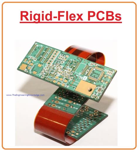
| Rigid-Flex PCBs | PCBs that combine a rigid board with flexible circuit layers | Laptops, gaming controllers, medical devices |
2. Medical Devices
PCBs are essential components in a variety of medical devices and equipment used for diagnostics, monitoring, and treatment. Some examples include:
- Patient monitoring systems
- Diagnostic imaging equipment like X-ray and ultrasound machines
- Surgical robotics and powered surgical tools
- Wearable health monitors and drug delivery devices
- Lab analysis instruments and automation equipment
- Medical implants like pacemakers and hearing aids
PCBs used in medical devices must meet strict quality and reliability standards to ensure proper functionality and patient safety. They often require speciality features like:
- Miniaturization for wearable and implantable devices
- High layer counts and dense interconnectivity
- Biocompatible materials that are non-toxic and resistant to bodily fluids
- Controlled impedance for high-speed data transmission
- Electromagnetic interference (EMI) shielding
- Ruggedized construction to withstand sterilization and frequent handling
3. Automotive Electronics
Modern vehicles contain dozens of electronic control units (ECUs) that manage various subsystems and functions. PCBs are core elements within these ECUs and other electronic modules in the car. Some automotive applications include:
- Engine control units and powertrains
- Transmission control modules
- Anti-lock braking systems (ABS)
- Advanced driver assistance systems (ADAS) with sensors and cameras
- Infotainment systems and instrument clusters
- Body control modules for functions like power windows and locks
- Battery management systems for electric vehicles
- Lighting and climate control systems
Automotive PCBs operate in harsh environments with extreme temperatures, vibration, and potential exposure to fluids and chemical solvents. Therefore, they must be designed and manufactured to high reliability standards like:
- Using high-temperature laminates and solder masks rated up to 150°C
- Incorporating heavy copper traces for high current applications
- Applying conformal coating to protect against moisture and contaminants
- Adhering to industry standards like ISOTS16949 and AEC-Q100
4. Industrial Equipment and Machinery
Industrial environments rely on advanced equipment and automated systems to power manufacturing lines, process control, robotics, and more. PCBs are integral to operating this machinery. Some industrial applications include:
- Programmable logic controllers (PLCs)
- Motor drives and servo controls
- Power converters and inverters
- Human machine interfaces (HMIs) and operator panels
- Sensors and data acquisition modules
- Networking and communication equipment
- Lighting and security systems
Like the automotive sector, industrial PCBs must withstand rugged conditions like extreme temperatures, high vibration, and exposure to dust and liquids. Additional PCB features for industrial use include:
- Thicker copper weights up to 20 oz for high current capacity
- Robust plated through-hole (PTH) construction
- Heatsinks and thermal vias for better heat dissipation
- Ruggedized connectors and enclosures
- Creepage and clearance spacing for high voltage circuits
- Conformance to UL, IPC, and ISO standards for safety and quality
5. Aerospace and Defense Systems
PCBs play a mission-critical role in aerospace and defense applications that demand the highest levels of reliability and durability. Some key areas include:
- Avionics and flight control systems
- Satellite and spacecraft electronics
- Radar and surveillance equipment
- Guidance and navigation systems
- Communication and encryption devices
- Electronic warfare and countermeasure technology
- Unmanned aerial vehicles (UAVs) and drones
To meet the stringent requirements for aerospace and defense, PCBs are often designed with speciality materials and manufacturing processes like:
- Polyimide laminates that withstand extreme temperature ranges
- Low-outgassing materials for vacuum environments
- Copper-clad aluminum cores for weight reduction
- High-speed, low-loss materials for RF/microwave circuits
- Tight tolerances and precision machining
- Extensive inspection and testing to military standards
6. Telecommunications Infrastructure
The telecommunications sector relies heavily on PCB-based hardware to enable the transmission, processing, and routing of voice and data signals. Some key telecom applications include:
- Wired and wireless network equipment
- Fiber optic transmission systems
- Cellular base stations and small cells
- Modems, routers, and gateways
- PBX and switching systems
- Satellite communications hardware
- Data center servers and storage systems
PCBs for telecommunications often deal with high-speed digital and RF/microwave signals, requiring careful design considerations like:
- Controlled impedance traces for signal integrity
- High layer counts up to 40+ layers for dense interconnectivity
- Low dielectric loss materials for high frequencies
- Fine line widths and tight tolerances
- Shielding and grounding techniques to minimize crosstalk and EMI
- HDI and microvias for miniaturization and high I/O density
- Thermal management for high-power applications

FAQ on PCB Applications
What are some emerging PCB applications to be aware of?
Some cutting-edge PCB applications that are rapidly growing include:
- 5G wireless infrastructure and edge devices
- Artificial intelligence (AI) and machine learning accelerators
- High-performance computing and data centers
- Advanced robotics and autonomous systems
- Electric and autonomous vehicles
- Renewable energy and smart grid technology
- Augmented reality/virtual reality (AR/VR) devices
- Medical wearables and point-of-care diagnostics
Are there any differences between PCBs for prototyping vs. production?
Yes, PCBs for prototyping are often designed for quick turnaround and lower cost, using common materials and standard specifications. They may have lower layer counts, larger feature sizes, and fewer speciality requirements compared to production boards.
In contrast, PCBs for volume production are optimized for manufacturability, reliability, and cost-effectiveness at scale. They often incorporate more advanced features and tighter tolerances that may not be necessary for prototypes.
How do I choose the right PCB manufacturer for my application?
When selecting a PCB fabricator, consider factors like:
- Their experience and capabilities in your specific application area
- Certifications and quality management systems they hold (e.g. ISO9001, IATF16949, AS9100)
- Prototyping and production volumes they can handle
- Types of materials, surface finishes, and speciality features they offer
- Their design for manufacturability (DFM) support and engineering expertise
- Lead times, pricing, and supply chain stability
- References from other customers in your industry
It’s best to work with a manufacturer that specializes in your application and can meet your technical and business requirements.
What are some common challenges when designing PCBs for different applications?
Some frequent challenges that PCB designers face across various applications include:
- Managing signal integrity and EMI at high frequencies
- Dissipating heat from high-power components
- Achieving high interconnect density and miniaturization
- Integrating multiple technologies (e.g. analog, digital, RF) on the same board
- Designing for harsh environmental conditions and reliability
- Optimizing layouts for manufacturability and cost
- Keeping up with rapidly evolving component technologies and industry standards
Partnering with an experienced PCB design firm and manufacturer can help overcome these challenges. Effective collaboration and a focus on DFM best practices are also key.
How can I stay up-to-date on the latest PCB application trends?
Some resources to stay informed about PCB industry trends include:
- Trade publications like Printed Circuit Design & Fab, SMT Magazine, and IEEE Spectrum
- Conferences and webinars hosted by industry associations like IPC and SMTA
- Online communities and forums for PCB designers and engineers
- Blogs and white papers from PCB software and manufacturing companies
- Analyst reports and market research on the electronics industry
Regularly engaging with these resources and networking with industry peers can help you stay current with the latest PCB technologies and application areas.

No responses yet