Introduction to PCB through-hole Technology
Printed Circuit Boards (PCBs) are essential components in modern electronic devices, providing a reliable and efficient means of connecting and integrating various electronic components. One crucial aspect of PCB production is the use of plated through-hole (PTH) technology. PTH is a method of creating electrical connections between the different layers of a PCB by drilling holes and plating them with a conductive material, typically copper.
What is PCB Through-Hole Technology?
PCB through-hole technology involves drilling holes through the PCB substrate and then plating the walls of these holes with a conductive material. This process creates a reliable electrical connection between the different layers of the PCB, allowing for the integration of components on both sides of the board.
The plating process typically involves the following steps:
- Drilling holes in the PCB substrate
- Cleaning and conditioning the hole walls
- Applying a thin layer of copper through electroless deposition
- Electroplating additional copper to achieve the desired thickness
- Applying a final finish, such as tin-lead, lead-free solder, or gold
Advantages of PCB Through-Hole Technology
PCB through-hole technology offers several advantages over other methods of connecting components on a PCB:
-
Mechanical Strength: PTH provides a strong mechanical connection between the components and the PCB, making the assembly more robust and resistant to vibration and shock.
-
Reliability: The plated holes create a reliable electrical connection between the layers of the PCB, reducing the risk of connection failures.
-
Compatibility: PTH is compatible with a wide range of components, including through-hole and surface-mount devices.
-
Thermal Management: The plated holes can help dissipate heat from components, improving the overall thermal management of the PCB.
The Role of PTH in PCB Manufacturing
PCB Design Considerations for Through-Hole Technology
When designing a PCB that incorporates through-hole technology, several factors must be considered to ensure optimal performance and manufacturability:
-
Hole Size: The diameter of the drilled holes should be appropriate for the component leads and the desired plating thickness. Smaller holes may be more challenging to plate and can increase manufacturing costs.
-
Pad Size: The pads surrounding the holes should be sized appropriately to accommodate the component leads and provide sufficient space for soldering.
-
Hole Placement: The placement of the holes should consider the routing of traces on the PCB and the overall component layout to minimize the risk of signal interference and ensure proper functionality.
-
Layer Stack-up: The number and arrangement of layers in the PCB Stack-Up should be designed to accommodate the required electrical connections and minimize the need for additional vias.
PCB Fabrication Process with PTH
The fabrication process for PCBs with plated through-holes involves several steps:
-
Drilling: Holes are drilled through the PCB substrate using a CNC drilling machine. The hole size and location are determined by the PCB design files.
-
Deburring: The drilled holes are deburred to remove any rough edges or debris that could interfere with the plating process.
-
Cleaning: The PCB is cleaned to remove any contaminants that could affect the plating process or the final product quality.
-
Electroless Copper Deposition: A thin layer of copper is deposited onto the hole walls through an electroless plating process. This layer acts as a conductive base for the subsequent electroplating step.
-
Electroplating: Additional copper is electroplated onto the hole walls to achieve the desired thickness and ensure a reliable electrical connection.
-
Final Finish: A final finish, such as tin-lead, lead-free solder, or gold, is applied to protect the copper and improve solderability.
Quality Control in PTH PCB Manufacturing
To ensure the quality and reliability of PCBs with plated through-holes, several quality control measures are implemented during the manufacturing process:
-
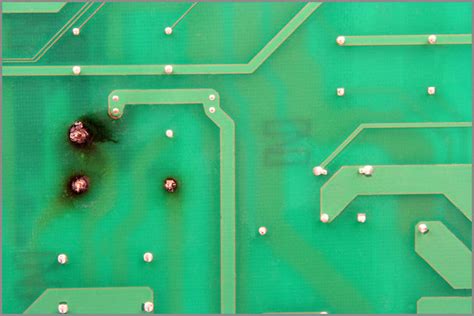
Visual Inspection: PCBs are visually inspected for defects such as incomplete plating, voids, or contamination.
-
Electrical Testing: Electrical tests, such as continuity and insulation resistance tests, are performed to verify the integrity of the electrical connections.
-
Microsectioning: Microsectioning involves cutting a cross-section of a plated hole and examining it under a microscope to assess the plating quality and thickness.
-
Thermal Stress Testing: PCBs may be subjected to thermal stress tests to evaluate their performance and reliability under varying temperature conditions.

Advancements in PCB Through-Hole Technology
High Aspect Ratio Drilling
High aspect ratio drilling refers to the ability to drill holes with a high ratio of depth to diameter. This technology enables the creation of smaller, more densely packed holes on a PCB, allowing for greater component density and miniaturization.
High aspect ratio drilling is achieved through the use of specialized drilling equipment and optimized drilling parameters, such as feed rates, spindle speeds, and drill bit geometry.
Via Filling
Via filling is a process in which the plated through-holes are filled with a non-conductive material, typically epoxy or a similar polymer. This process offers several benefits:
-
Improved Signal Integrity: Filled vias can help reduce signal reflections and crosstalk, improving the overall signal integrity of the PCB.
-
Enhanced Thermal Management: Filled vias can provide a thermal path for heat dissipation, helping to manage the temperature of the PCB and its components.
-
Increased Mechanical Strength: Filled vias can improve the mechanical strength of the PCB, particularly in areas with a high density of holes.
Microvias
Microvias are small, laser-drilled holes that provide electrical connections between the layers of a PCB. These vias are typically smaller than those created through mechanical drilling, with diameters ranging from 50 to 150 microns.
Microvias offer several advantages over traditional mechanically drilled holes:
-
Higher Density: The smaller size of microvias allows for greater hole density and more compact PCB designs.
-
Improved Signal Integrity: The reduced size and length of microvias can help minimize signal reflections and improve overall signal integrity.
-
Cost Reduction: Microvias can reduce the need for multiple lamination cycles, leading to lower production costs and shorter lead times.

FAQs
1. What is the difference between through-hole and surface-mount technology?
Through-hole technology involves inserting component leads through holes drilled in the PCB and soldering them on the opposite side. Surface-mount technology (SMT) involves placing components directly onto the surface of the PCB and soldering them in place. SMT allows for smaller components and higher component density, while through-hole technology offers greater mechanical strength and reliability.
2. Can through-hole and surface-mount components be used on the same PCB?
Yes, it is possible to use both through-hole and surface-mount components on the same PCB. This is known as a mixed-technology or hybrid PCB. Mixed-technology PCBs offer the benefits of both through-hole and surface-mount technologies, allowing for greater design flexibility and optimized performance.
3. What is the purpose of applying a final finish to the plated through-holes?
The final finish applied to plated through-holes serves several purposes:
-
Protection: The final finish protects the copper plating from oxidation and corrosion, ensuring the long-term reliability of the electrical connections.
-
Solderability: Finishes such as tin-lead or lead-free solder improve the solderability of the holes, making it easier to attach components during the assembly process.
-
Aesthetics: Some finishes, such as gold, can enhance the visual appearance of the PCB.
4. How does the aspect ratio of a drilled hole affect the PCB manufacturing process?
The aspect ratio of a drilled hole refers to the ratio of the hole’s depth to its diameter. Higher aspect ratios can pose challenges in the PCB manufacturing process, particularly during the plating stage. As the aspect ratio increases, it becomes more difficult to ensure even plating coverage and maintain the desired plating thickness. High aspect ratio holes may require specialized drilling equipment and optimized plating processes to achieve the required quality and reliability.
5. What are the advantages of using microvias in PCB design?
Microvias offer several advantages in PCB design:
-
Higher Density: The smaller size of microvias allows for greater hole density and more compact PCB layouts, enabling the design of smaller and more complex electronic devices.
-
Improved Signal Integrity: The reduced size and length of microvias can help minimize signal reflections and improve overall signal integrity, particularly in high-speed and high-frequency applications.
-
Cost Reduction: Microvias can reduce the need for multiple lamination cycles, leading to lower production costs and shorter lead times compared to traditional mechanically drilled holes.
-
Design Flexibility: Microvias can be placed in locations where mechanical drilling is not feasible, such as directly under components, offering greater design flexibility and improved space utilization.

Conclusion
Plated through-hole technology plays a critical role in the production of reliable and high-quality PCBs. By providing strong mechanical connections and reliable electrical paths between the layers of a PCB, PTH enables the integration of a wide range of electronic components and ensures the proper functioning of electronic devices.
As PCB designs continue to evolve and become more complex, advancements in through-hole technology, such as high aspect ratio drilling, via filling, and microvias, are enabling the development of smaller, more densely packed, and higher-performance electronic devices.
By understanding the importance of PTH in PCB manufacturing and staying informed about the latest advancements in this technology, PCB designers and manufacturers can create innovative and reliable electronic products that meet the ever-increasing demands of the modern world.
| Aspect | Through-Hole Technology | Surface-Mount Technology |
|---|---|---|
| Component Mounting | Leads inserted through holes | Components placed directly on surface |
| Hole Drilling | Required | Not required |
| Solder Joint Strength | Strong | Weaker |
| Component Density | Lower | Higher |
| PCB Size | Larger | Smaller |
| Manufacturing Cost | Higher | Lower |
| Rework and Repair | Easier | More challenging |
No responses yet