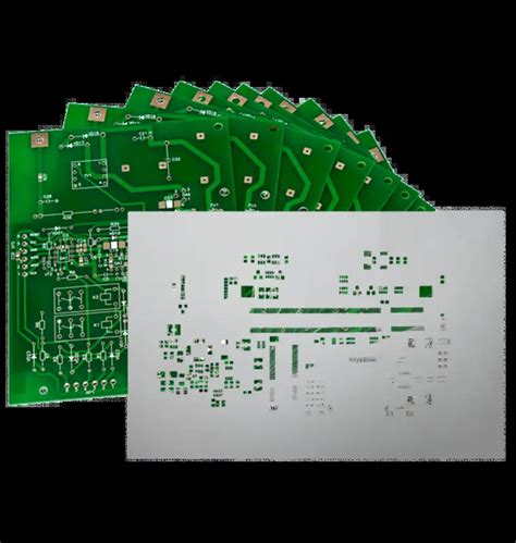
What is a PCB Stencil?
A PCB (Printed Circuit Board) stencil is a thin sheet of metal, usually stainless steel, with laser-cut openings that correspond to the pads on a PCB. The stencil is used to apply solder paste onto the PCB pads before components are placed and the board is sent through a reflow oven for soldering. This process ensures precise and consistent application of solder paste, which is crucial for the proper functioning of the electronic device.
Types of PCB Stencils
There are two main types of PCB stencils:
-
Framed Stencils: These stencils have a metal frame around the perimeter, which provides rigidity and makes them easier to handle. Framed stencils are more durable and suitable for high-volume production.
-
Frameless Stencils: Also known as prototype stencils, these are cheaper and faster to produce. They are ideal for low-volume production or prototyping.
Why Use a PCB Stencil?
Using a PCB stencil offers several advantages:
-
Precision: Stencils ensure accurate and consistent solder paste application, which is essential for surface mount technology (SMT) components with fine pitch leads.
-
Efficiency: Stencils allow for faster application of solder paste compared to manual methods, making them ideal for high-volume production.
-
Cost-effective: Although the initial cost of a stencil may be higher, it saves time and reduces waste in the long run, making it a cost-effective solution.
How to Choose the Right PCB Stencil
When selecting a PCB stencil, consider the following factors:
Stencil Thickness
The thickness of the stencil determines the amount of solder paste deposited on the pads. The ideal thickness depends on the size and pitch of the components.
| Component Pitch | Recommended Stencil Thickness |
|---|---|
| 0.3 mm | 0.1 mm |
| 0.4 mm | 0.12 mm |
| 0.5 mm | 0.15 mm |
| 0.8 mm | 0.2 mm |
Aperture Design
The aperture design refers to the shape and size of the openings in the stencil. The most common aperture designs are:
- Square: Suitable for most SMD pads.
- Rounded: Used for BGA (Ball Grid Array) and QFN (Quad Flat No-lead) packages to prevent bridging.
- Oblong: Used for fine pitch components to prevent bridging.
Stencil Material
Stainless steel is the most common material for PCB stencils due to its durability and precision. However, other materials like nickel and polyimide can also be used for specific applications.

Stencil Printing Process
The stencil printing process involves the following steps:
-
Alignment: The stencil is aligned with the PCB using fiducial marks or pins.
-
Solder Paste Application: Solder paste is placed on the stencil and spread across the openings using a squeegee.
-
Inspection: The PCB is inspected for proper solder paste application and any defects are corrected.
-
Component Placement: The components are placed on the PCB using a pick-and-place machine or manually.
-
Reflow: The PCB is sent through a reflow oven to melt the solder paste and form a permanent connection between the components and the board.
Stencil Maintenance and Cleaning
To ensure the longevity and performance of your PCB stencil, regular maintenance and cleaning are essential.
Cleaning Methods
-
Manual Cleaning: Use a lint-free cloth and a suitable solvent (e.g., isopropyl alcohol) to wipe the stencil clean.
-
Ultrasonic Cleaning: Place the stencil in an ultrasonic cleaner with a cleaning solution for a thorough clean.
-
Automated Cleaning: Use a stencil cleaning machine for efficient and consistent cleaning, especially in high-volume production.
Storage
Store your stencils in a clean, dry environment to prevent corrosion and damage. Use a stencil storage rack or a protective case to keep them organized and easily accessible.
Frequently Asked Questions (FAQ)
-
What is the difference between a PCB stencil and a solder paste screen?
A PCB stencil and a solder paste screen serve the same purpose of applying solder paste onto PCB pads. However, a stencil is made of metal (usually stainless steel), while a screen is made of a mesh material (usually polyester or stainless steel). -
Can I reuse a PCB stencil?
Yes, PCB stencils can be reused multiple times with proper cleaning and maintenance. However, over time, the stencil may wear out or become damaged, affecting the quality of the solder paste application. -
How do I know if my PCB stencil is worn out?
Signs of a worn-out stencil include: - Inconsistent solder paste application
- Damaged or deformed apertures
-
Visible wear and tear on the stencil surface
-
Can I use a PCB stencil for through-hole components?
PCB stencils are primarily used for surface mount components. For through-hole components, solder paste is not typically used, and the components are soldered manually or using a wave soldering machine. -
How do I store my PCB stencils?
Store your PCB stencils in a clean, dry environment to prevent corrosion and damage. Use a stencil storage rack or a protective case to keep them organized and easily accessible. Avoid storing stencils in humid or dusty areas, as this can affect their performance and longevity.
Conclusion
PCB stencils are an essential tool in the electronics manufacturing process, ensuring precise and consistent solder paste application for surface mount components. By understanding the types of stencils, their benefits, and how to choose the right one for your project, you can optimize your PCB assembly process and achieve better results. Regular maintenance and cleaning of your stencils will also help extend their lifespan and maintain the quality of your solder paste application.
As the electronics industry continues to evolve, with smaller components and more complex designs, the importance of PCB stencils will only continue to grow. By staying up-to-date with the latest technologies and best practices in stencil design and usage, you can ensure that your PCB assembly process remains efficient, cost-effective, and yields high-quality results.

No responses yet