PCB design Pitfalls to Avoid for Successful Manufacturing
Printed circuit board (PCB) design is a complex process that requires careful planning and attention to detail. Even experienced designers can fall victim to common PCB design pitfalls that lead to manufacturing issues, delays, and increased costs. In this article, we’ll explore ten of the most common problems encountered in PCB design and how to avoid them.
1. Incorrect Component Footprints
One of the most frequent issues in PCB design is using incorrect component footprints. This can happen when designers rely on outdated or inaccurate component libraries, or when they fail to double-check the dimensions and pin assignments of the components they are using.
To avoid this pitfall:
– Always use up-to-date component libraries from reliable sources
– Verify component footprints against manufacturer datasheets
– Double-check pin assignments and orientations
2. Inadequate Clearance and Creepage
Clearance refers to the minimum distance between two conductive parts, while creepage is the shortest path between two conductive parts along the surface of the insulating material. Insufficient clearance and creepage can lead to short circuits, arcing, and other reliability issues.
To ensure adequate clearance and creepage:
– Follow the recommended guidelines for your PCB’s voltage and environment
– Use design rule checks (DRC) to verify clearance and creepage distances
– Consider using conformal coating or potting for additional insulation
3. Improper Trace Width and Spacing
Trace width and spacing play a critical role in signal integrity, power delivery, and manufacturability. Traces that are too narrow can cause excessive resistance and heating, while traces that are too close together can lead to crosstalk and electromagnetic interference (EMI).
To optimize trace width and spacing:
– Calculate the appropriate trace width based on current requirements and temperature rise
– Follow the recommended trace spacing guidelines for your PCB’s layer count and manufacturing capabilities
– Use Impedance Calculators to determine the optimal trace geometry for controlled impedance designs
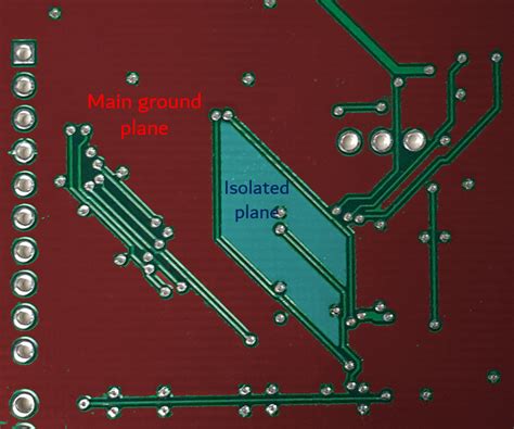
4. Ineffective Power and Ground Planes
Power and ground planes are essential for providing low-impedance power delivery and reducing EMI. However, poorly designed power and ground planes can lead to voltage drops, ground loops, and other issues that can compromise the performance and reliability of the PCB.
To create effective power and ground planes:
– Use solid copper pours instead of gridded planes
– Minimize the number of cuts and splits in the planes
– Use stitching vias to connect planes on different layers
– Place Decoupling Capacitors close to power pins
5. Insufficient Via Size and Spacing
Vias are used to connect traces on different layers of the PCB. If the vias are too small or too close together, they can be difficult to manufacture and may cause reliability issues. On the other hand, vias that are too large can consume valuable board space and increase manufacturing costs.
To optimize via size and spacing:
– Follow the recommended via size and spacing guidelines for your PCB’s manufacturing capabilities
– Use via tenting or filling to improve reliability and reduce solder wicking
– Consider using microvias for high-density designs
6. Incorrect Layer Stack-up
The layer stack-up of a PCB determines the arrangement of copper layers, insulating materials, and plated through-holes. An incorrect layer stack-up can lead to signal integrity issues, impedance mismatches, and manufacturability problems.
To create a correct layer stack-up:
– Work with your PCB manufacturer to select the appropriate materials and thicknesses
– Follow the recommended layer arrangement for your PCB’s application and manufacturing capabilities
– Use impedance calculators to determine the optimal dielectric thickness and trace geometry
7. Lack of Design for Manufacturing (DFM) Considerations
Design for Manufacturing (DFM) is the practice of designing PCBs with the manufacturing process in mind. Neglecting DFM considerations can lead to increased manufacturing costs, lower yields, and longer lead times.
To incorporate DFM into your PCB design process:
– Follow the recommended design rules for your PCB manufacturer
– Use DFM analysis tools to identify and correct potential manufacturing issues
– Communicate with your manufacturer early in the design process to ensure compatibility
8. Ignoring Signal Integrity and EMC
Signal integrity and electromagnetic compatibility (EMC) are critical aspects of PCB design that ensure the proper functioning of the circuit and compliance with regulatory standards. Ignoring these factors can lead to crosstalk, reflections, ringing, and EMI issues.
To address signal integrity and EMC:
– Use appropriate termination and matching techniques for high-speed signals
– Minimize the loop area of critical signal paths
– Use ground planes and shielding to reduce EMI
– Perform Signal integrity simulations and EMC testing to validate the design
9. Improper Component Placement
Component placement is a key factor in determining the performance, reliability, and manufacturability of a PCB. Poor component placement can lead to signal integrity issues, thermal problems, and assembly difficulties.
To optimize component placement:
– Group related components together to minimize trace lengths and simplify routing
– Place heat-generating components away from temperature-sensitive devices
– Consider the assembly process and ensure adequate clearance for pick-and-place machines and soldering equipment
– Use design for assembly (DFA) guidelines to improve manufacturability
10. Insufficient Documentation and Version Control
PCB design is an iterative process that involves multiple revisions and collaborators. Insufficient documentation and version control can lead to confusion, errors, and delays in the design and manufacturing process.
To ensure proper documentation and version control:
– Use a version control system to track changes and collaborate with team members
– Maintain a clear and consistent naming convention for design files and revisions
– Create detailed assembly drawings, schematics, and bill of materials (BOM)
– Communicate any changes or updates to the manufacturer in a timely manner
By being aware of these common PCB design pitfalls and taking steps to avoid them, designers can create more reliable, manufacturable, and cost-effective PCBs.
PCB Design Pitfall FAQs
1. What is the most common mistake in PCB design?
One of the most common mistakes in PCB design is using incorrect component footprints. This can lead to assembly issues and require costly rework.
2. How can I ensure adequate clearance and creepage in my PCB design?
To ensure adequate clearance and creepage, follow the recommended guidelines for your PCB’s voltage and environment, use design rule checks (DRC) to verify distances, and consider using conformal coating or potting for additional insulation.
3. What is the importance of a correct layer stack-up in PCB design?
A correct layer stack-up is essential for maintaining signal integrity, achieving the desired impedance, and ensuring manufacturability. An incorrect layer stack-up can lead to performance issues and manufacturing problems.
4. How can I incorporate Design for Manufacturing (DFM) into my PCB design process?
To incorporate DFM into your PCB design process, follow the recommended design rules for your PCB manufacturer, use DFM analysis tools to identify potential issues, and communicate with your manufacturer early in the design process.
5. Why is proper documentation and version control important in PCB design?
Proper documentation and version control are crucial for tracking changes, collaborating with team members, and communicating with manufacturers. Insufficient documentation and version control can lead to errors, delays, and increased costs in the design and manufacturing process.
| PCB Design Pitfall | Consequences | Prevention Techniques |
|---|---|---|
| Incorrect Component Footprints | Assembly issues, costly rework | Use up-to-date libraries, verify footprints, double-check pin assignments |
| Inadequate Clearance and Creepage | Short circuits, arcing, reliability issues | Follow voltage and environment guidelines, use DRC, consider conformal coating |
| Improper Trace Width and Spacing | Excessive resistance, heating, crosstalk, EMI | Calculate appropriate width, follow spacing guidelines, use impedance calculators |
| Ineffective Power and Ground Planes | Voltage drops, ground loops, EMI | Use solid copper pours, minimize cuts and splits, use stitching vias, place decoupling capacitors |
| Insufficient Via Size and Spacing | Manufacturing difficulties, reliability issues, increased costs | Follow manufacturing guidelines, use via tenting or filling, consider microvias |
By understanding and addressing these common PCB design pitfalls, designers can create more robust, reliable, and manufacturable PCBs, ultimately saving time and money in the development process.
No responses yet