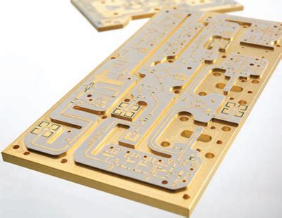
What is a Teflon PCB?
A Teflon PCB, also known as a PTFE (polytetrafluoroethylene) PCB, is a specialized type of printed circuit board that utilizes Teflon as the base material instead of the more commonly used FR-4. Teflon is a synthetic fluoropolymer known for its excellent dielectric properties, low dissipation factor, and high thermal stability. These characteristics make Teflon PCBs an ideal choice for high-frequency applications, such as radar systems, satellite communications, and microwave devices.
Advantages of Teflon PCBs
- High dielectric constant and low dissipation factor
- Excellent thermal stability
- Low moisture absorption
- High chemical resistance
- Low coefficient of friction
Applications of Teflon PCBs
- High-frequency communications
- Microwave devices
- Radar systems
- Aerospace and defense electronics
- Medical equipment
Properties of Teflon
Teflon, or PTFE, is a fluoropolymer composed of carbon and fluorine atoms. It was accidentally discovered by Roy Plunkett, a chemist at DuPont, in 1938. Since then, it has found numerous applications due to its unique properties.
Physical Properties
- Melting point: 327°C (620°F)
- Density: 2.2 g/cm³
- Tensile strength: 20-35 MPa
- Elongation at break: 200-400%
Electrical Properties
- Dielectric constant: 2.1 (at 1 MHz)
- Dissipation factor: 0.0002 (at 1 MHz)
- Volume resistivity: > 10¹⁸ Ω·cm
- Dielectric strength: 60-173 kV/mm
Thermal Properties
- Thermal conductivity: 0.25 W/(m·K)
- Coefficient of thermal expansion: 100-160 ppm/°C
- Continuous service temperature: -200 to 260°C

Manufacturing Process of Teflon PCBs
The manufacturing process of Teflon PCBs is similar to that of standard FR-4 PCBs, with a few key differences due to the unique properties of Teflon.
Substrate Preparation
- Teflon laminate is cut to the desired size.
- Copper foil is laminated onto the Teflon substrate using high temperature and pressure.
- The copper-clad Teflon substrate is cleaned and inspected for defects.
Circuit Patterning
- A photoresist layer is applied to the copper surface.
- The circuit pattern is transferred to the photoresist using photolithography.
- The exposed copper is etched away, leaving the desired circuit pattern.
- The remaining photoresist is removed.
Drilling and Plating
- Holes are drilled through the Teflon PCB for component mounting and interconnections.
- The holes are plated with copper to create electrical connections between layers.
- Additional copper is plated onto the surface to increase the thickness of the tracks and pads.
Solder Mask and Silkscreen
- A solder mask is applied to the PCB to protect the copper traces and prevent short circuits.
- Silkscreen legends and symbols are printed onto the PCB for component identification and assembly guidance.
Surface Finishing
- A surface finish, such as ENIG (Electroless Nickel Immersion Gold) or HASL (Hot Air Solder Leveling), is applied to the exposed copper areas to protect them from oxidation and improve solderability.
- The PCB is cleaned, inspected, and packaged for shipping.

Design Considerations for Teflon PCBs
When designing Teflon PCBs, there are several factors to consider to ensure optimal performance and manufacturability.
Material Selection
- Choose the appropriate Teflon laminate grade based on the application requirements, such as dielectric constant, dissipation factor, and thermal stability.
- Consider the copper foil thickness and surface roughness for high-frequency applications.
Trace Width and Spacing
- Use appropriate trace widths and spacing to minimize signal loss and crosstalk.
- Calculate the characteristic impedance of the traces based on the dielectric constant of the Teflon substrate and the trace dimensions.
Via Design
- Minimize the number of vias to reduce signal reflections and losses.
- Use blind and buried vias when necessary to improve signal integrity and reduce board size.
Thermal Management
- Consider the thermal conductivity of Teflon when designing for high-power applications.
- Use thermal vias and heat sinks to dissipate heat from critical components.
Mechanical Considerations
- Account for the lower mechanical strength and higher thermal expansion of Teflon compared to FR-4.
- Use appropriate mounting techniques and strain relief to minimize mechanical stress on the PCB.

Teflon PCB vs. FR-4 PCB
Teflon PCBs offer several advantages over traditional FR-4 PCBs, particularly in high-frequency applications. However, they also have some disadvantages that should be considered when choosing between the two materials.
| Property | Teflon PCB | FR-4 PCB |
|---|---|---|
| Dielectric Constant | 2.1 (at 1 MHz) | 4.5 (at 1 MHz) |
| Dissipation Factor | 0.0002 (at 1 MHz) | 0.02 (at 1 MHz) |
| Thermal Stability | High | Moderate |
| Moisture Absorption | Low | Moderate |
| Mechanical Strength | Low | High |
| Cost | High | Low |
Frequently Asked Questions (FAQ)
1. What is the difference between Teflon and PTFE?
Teflon is a brand name for PTFE (polytetrafluoroethylene), which is a synthetic fluoropolymer. While all Teflon is PTFE, not all PTFE is Teflon, as there are other manufacturers of PTFE materials.
2. Can Teflon PCBs be used for low-frequency applications?
Yes, Teflon PCBs can be used for low-frequency applications, but they may not offer significant advantages over FR-4 PCBs in these cases. The benefits of Teflon PCBs are most apparent in high-frequency applications.
3. Are Teflon PCBs more expensive than FR-4 PCBs?
Yes, Teflon PCBs are generally more expensive than FR-4 PCBs due to the higher cost of the Teflon laminate and the specialized manufacturing processes required.
4. How do Teflon PCBs handle high temperatures?
Teflon PCBs have excellent thermal stability and can operate continuously at temperatures ranging from -200°C to 260°C. This makes them suitable for applications that involve high temperatures or extreme temperature fluctuations.
5. Can Teflon PCBs be assembled using standard soldering techniques?
Yes, Teflon PCBs can be assembled using standard soldering techniques, such as reflow soldering and wave soldering. However, the lower surface energy of Teflon may require the use of special fluxes or surface treatments to ensure proper solder wetting.
Conclusion
Teflon PCBs offer unique advantages in high-frequency applications due to their excellent dielectric properties, low dissipation factor, and high thermal stability. While they may be more expensive than traditional FR-4 PCBs, their performance benefits can justify the added cost in demanding applications such as radar systems, satellite communications, and microwave devices.
When designing Teflon PCBs, it is essential to consider factors such as material selection, trace dimensions, via design, thermal management, and mechanical considerations to ensure optimal performance and reliability. By understanding the properties and manufacturing processes of Teflon PCBs, designers can leverage the material’s strengths to create high-performance electronic systems.
No responses yet