Introduction to the TDA2822 Audio Amplifier IC
The TDA2822 is a popular dual low-voltage power amplifier IC manufactured by ST Microelectronics. It is designed for use in battery-powered portable audio devices such as radios, MP3 players, and small stereo systems. The TDA2822 provides good audio quality with low distortion while operating efficiently from a low supply voltage.
Key features of the TDA2822 include:
- Dual bridge-tied load (BTL) amplifier configuration
- Low supply voltage range: 1.8V to 6V
- Low quiescent current: 4mA per channel
- High output power: up to 1.2W per channel into 8Ω at 6V
- Low distortion: 0.1% THD at 0.5W output
- Thermal protection and short circuit protection
- Small 8-pin DIP or SOIC package
The TDA2822’s combination of good audio performance, low power consumption, and small size make it a popular choice for battery-powered audio projects. It is simple to use and requires few external components.
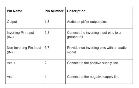
TDA2822 Pinout and Pin Functions
The TDA2822 is available in 8-pin plastic DIP and surface-mount SOIC packages. The pinout is as follows:
| Pin | Function |
|---|---|
| 1 | OUT1 |
| 2 | IN1 |
| 3 | GND |
| 4 | IN2 |
| 5 | OUT2 |
| 6 | VS |
| 7 | BYPASS |
| 8 | STBY |
A brief description of each pin’s function:
- OUT1, OUT2: Amplifier outputs. Connect directly to speakers or through DC blocking capacitors.
- IN1, IN2: Amplifier inputs. Typically connected to audio source through coupling capacitors.
- GND: Ground. All grounds (input, output, power) connect here.
- VS: Positive power supply. Must be between 1.8V and 6V.
- BYPASS: Connects to VS through a Bypass Capacitor to reduce power supply noise.
- STBY: Standby control pin. Pulling this pin low (<0.7V) puts the chip in a low-power standby state. Leave floating or connect to VS for normal operation.

Absolute Maximum Ratings
The TDA2822 is designed to operate within the following limits:
| Parameter | Value | Units |
|---|---|---|
| Supply Voltage (VS) | 7 | V |
| Input Voltage (IN1, IN2) | VS | V |
| Operating Temperature Range | -40 to +85 | °C |
| Power Dissipation (Ta ≤ 75°C) | 1 | W |
Exceeding these limits may cause permanent damage to the device. Care should be taken to ensure that the power supply voltage, input voltages, and device temperature remain within acceptable ranges during operation.

Electrical Characteristics
The following table summarizes key electrical characteristics of the TDA2822, measured under typical operating conditions (VS = 6V, f = 1 kHz, RL = 8Ω, unless otherwise noted):
| Parameter | Symbol | Conditions | Min | Typ | Max | Unit |
|---|---|---|---|---|---|---|
| Quiescent Current (total) | IQ | 8 | 14 | mA | ||
| Quiescent Current (per channel) | IQ | 4 | 7 | mA | ||
| Output Power (per channel) | PO | THD = 10%, f = 1 kHz, RL = 8Ω | 1.1 | 1.3 | W | |
| Total Harmonic Distortion | THD | PO = 0.5 W | 0.1 | 0.5 | % | |
| Voltage Gain | VG | 35 | 40 | 45 | dB | |
| Channel Separation | CS | f = 1 kHz | 55 | dB | ||
| Input Resistance | RIN | 50 | kΩ | |||
| Standby Current | ISTBY | VSTBY ≤ 0.7V | 1 | 10 | µA |
These specifications demonstrate the TDA2822’s high output power, low distortion, and good channel separation, while maintaining low quiescent current and compatibility with low supply voltages.

Application Circuit and Component Selection
A typical application circuit for the TDA2822 is shown below:
        +VS
         |
 .-------+-------.
 |               |
 |              === C5
 |               |
 |     .----+----'
 |     |    |
 |     |   === C6
 |    .+-.  |
 |    |  |  |
-+----+  |  |  .------.
 |    '+-'  |  |      |
 |     |    |  |      |
 |    C4   R4  |     === C1
 |     |    |  |      |
 |    .+.   |  '------+------.
 |    | |   |         |      |
 |   R3'   R2         |     ,+,
 |    | |   |        .+.    ///
 |    '+'   |        | |   (8Ω)
 |     |    |       C3'     \\\
 '-----+-. .+.       | |     '-'
IN1     | | | |      '+' TDA2822
GND  ---' | | '---+---+---+---+----
IN2   ----' |     |   |   |   |
       R1   '-----)---)---)---)---
               OUT1  VS GND   STBY
Recommended component values:
- C1, C3: 220µF electrolytic capacitors. Provide DC blocking and filtering for speaker outputs.
- C4: 0.1µF ceramic capacitor. Input coupling capacitor to block DC.
- C5: 100µF electrolytic capacitor. Bulk power supply filter capacitor.
- C6: 0.1µF ceramic capacitor. High-frequency power supply bypass capacitor.
- R1, R2: 10kΩ resistors. Set input bias and provide a path for input bias currents.
- R3: 1Ω resistor. Bootstrap resistor to improve output voltage swing and reduce distortion.
- R4: 10Ω resistor. Reduces high frequency oscillation and improves stability.
The input coupling capacitor C4 and input bias resistors R1/R2 form a high-pass filter with a cutoff frequency of:
f = 1 / (2π × R × C)
  ≈ 1 / (2π × 10kΩ × 0.1µF)
  ≈ 160 Hz
This rolls off low frequencies below 160 Hz to reduce low-frequency noise and prevent speaker overdrive at low frequencies.
The output filter capacitors C1 and C3 form a low-pass filter with the speaker load resistance. With an 8Ω speaker load, the cutoff frequency is:
f = 1 / (2π × R × C)
  ≈ 1 / (2π × 8Ω × 220µF)
  ≈ 90 Hz
This rolls off high frequencies to reduce EMI while allowing most of the audio band to pass.
PCB Layout Considerations
Proper PCB layout is important to achieve optimal performance from the TDA2822. Some key layout guidelines:
- Place the TDA2822 close to the speaker outputs to minimize trace length and inductance.
- Use wide, short traces for power supply and output connections to minimize resistance.
- Provide a solid ground plane on the component layer and keep analog and digital grounds separate.
- Place the input coupling capacitor C4 close to the input pins to minimize noise pickup.
- Place the power supply bypass capacitor C6 as close as possible to the VS and GND pins.
- Keep high-current output traces away from sensitive input traces to avoid crosstalk.
- Use a star ground topology with all grounds returning to a single point near the power input.
Proper layout minimizes EMI, reduces noise, and ensures stable operation at high output power.
Thermal Considerations and Heat Sinking
The TDA2822 has built-in thermal protection that activates when the die temperature exceeds 150°C. However, for reliable operation, it is recommended to keep the die temperature below 125°C.
The power dissipated in the TDA2822 can be calculated as:
PD = (VS - VO) × IL
Where:
– PD is power dissipation
– VS is supply voltage
– VO is output voltage (≈ VS/2)
– IL is load current
At the maximum output power of 1.2W into 8Ω from a 6V supply:
IL = √(PO / RL)
   = √(1.2W / 8Ω)
   ≈ 390 mA

PD = (6V - 6V/2) × 0.39A
   = 1.17W
Without a heatsink, the TDA2822’s junction-to-ambient thermal resistance (RθJA) is 80°C/W. At 1.17W dissipation, the junction temperature rise would be:
ΔTJ = PD × RθJA
    = 1.17W × 80°C/W
    = 94°C
Adding the maximum ambient temperature of 85°C gives a junction temperature of 179°C, exceeding the 150°C limit.
To keep the junction temperature below 125°C with an 85°C ambient, the required thermal resistance is:
RθJA = (TJ(max) - TA) / PD
     = (125°C - 85°C) / 1.17W
     = 34°C/W
A small heatsink can be added to reduce RθJA and keep the TDA2822 within its thermal limits.
Treble Boost Circuit
The TDA2822 can be modified to provide an adjustable treble boost, which can help compensate for high-frequency roll-off in small speakers. The treble boost circuit adds a high-pass filter to the amplifier’s feedback network, increasing the gain at high frequencies.
        .-------+-------.
        |       |       |
       C5      R6      R5
        |       |       |
       ===   .--+--..---+----.
        |    |     ||        |
       ===   |    C7'        |
        |    |     ||        |
        |   C4'    ||       +-> OUT
        |    |     +'      -+
        |    |     ||   R4' |
       |   R3'    R2'       |
       |    |     ||        |
      |    |     ||        |
IN ->-+----|-----+---+--+---|---
             R1'      |  |
                     -+  +-
                      '  '
                      GND
Recommended component values:
- R2′: 10kΩ
- R3′: 1kΩ
- R4′: 100Ω
- R5: 10kΩ potentiometer
- R6: 3.3kΩ
- C4′: 0.1µF
- C7′: 4.7nF
The treble boost amount is adjustable from 0 to approximately +10 dB at 10 kHz by varying potentiometer R5. Capacitor C7′ sets the frequency at which the boost begins, while resistors R5 and R6 set the maximum boost amount.
FAQ
Q: What is the maximum supply voltage for the TDA2822?
A: The absolute maximum supply voltage is 7V. For normal operation, the supply voltage should be kept between 1.8V and 6V.
Q: How much output power can the TDA2822 deliver?
A: The TDA2822 can deliver up to 1.2W per channel into an 8Ω load with a 6V supply. Output power is lower with lower supply voltages or higher load impedances.
Q: What is the minimum load impedance for the TDA2822?
A: The TDA2822 is stable with load impedances as low as 4Ω. However, lower impedances result in higher load currents and increased power dissipation in the IC, which may require heatsinking to avoid thermal shutdown.
Q: Can the TDA2822 be used in a single-supply configuration?
A: Yes, the TDA2822 is designed for single-supply operation. The minimum supply voltage is 1.8V.
Q: What is the function of the STBY pin?
A: The STBY pin allows the TDA2822 to be put into a low-power standby mode when not in use. Pulling the STBY pin below 0.7V reduces the supply current to less than 10µA. Leaving the STBY pin floating or connected to VS enables normal operation.
Conclusion
The TDA2822 is a versatile and easy-to-use dual audio power amplifier IC that delivers good performance from a low supply voltage. Its low quiescent current and shutdown mode make it well-suited for battery-powered applications, while its low distortion and high output power provide good audio quality. With proper component selection, PCB layout, and heatsinking, the TDA2822 is an excellent choice for a wide range of portable and low-power audio applications.
No responses yet