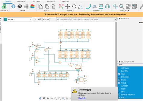
The Importance of Syncing Schematics and PCB Layouts
Syncing your schematics and PCB layouts is essential for several reasons:
-
Error Reduction: When your schematics and PCB layouts are in sync, you minimize the chances of introducing errors during the design process. Inconsistencies between the two can lead to issues such as incorrect component placement, signal integrity problems, and manufacturability challenges.
-
Improved Efficiency: By ensuring that your schematics and PCB layouts are always in sync, you can work more efficiently. Changes made in the schematic are automatically reflected in the PCB layout, reducing the need for manual updates and saving valuable time.
-
Faster Iterations: With synchronized schematics and PCB layouts, making revisions and iterating on your design becomes a smoother process. You can quickly incorporate feedback, make necessary adjustments, and move forward with confidence, knowing that your schematic and layout are aligned.
-
Better Collaboration: Syncing your schematics and PCB layouts facilitates better collaboration among team members. When everyone is working with the same updated information, communication becomes clearer, and the chances of misunderstandings or conflicting changes are minimized.
Best Practices for Syncing Schematics and PCB Layouts
To effectively sync your schematics and PCB layouts, consider the following best practices:
1. Use Integrated Design Tools
Invest in integrated design tools that provide a seamless workflow between schematic capture and PCB layout. These tools often offer features like cross-probing, real-time synchronization, and automatic updating of component footprints and pin assignments. Some popular integrated design tools include:
- Altium Designer
- Cadence OrCAD
- Mentor Graphics PADS
- KiCad
2. Establish a Clear Design Flow
Define a clear and consistent design flow that outlines the steps involved in creating and updating your schematics and PCB layouts. This flow should include tasks such as:
- Schematic capture
- Component selection and symbol creation
- Footprint creation and association
- PCB layout and routing
- Design rule checks (DRC) and electrical rule checks (ERC)
- Generating manufacturing files
By following a well-defined design flow, you can ensure that everyone on your team is on the same page and that the necessary steps are taken to keep your schematics and PCB layouts in sync.
3. Utilize Version Control
Implement version control systems to manage your schematic and PCB layout files. Version control allows you to track changes, revert to previous versions if needed, and collaborate with team members without the risk of overwriting each other’s work. Some popular version control systems for electronics design include:
- Git
- SVN (Subversion)
- Perforce
4. Regularly Review and Update
Schedule regular reviews of your schematics and PCB layouts to ensure that they remain in sync throughout the design process. These reviews should involve checking for consistency, verifying component footprints, and ensuring that any changes made in the schematic are properly reflected in the PCB layout.
5. Communicate and Collaborate
Foster open communication and collaboration among team members involved in the design process. Encourage regular discussions, design reviews, and feedback sessions to identify and address any discrepancies between the schematics and PCB layouts. Use collaborative tools like shared workspaces, real-time chat, and issue tracking systems to facilitate effective communication.
Common Challenges and Solutions
Despite best efforts, challenges can arise when syncing schematics and PCB layouts. Here are some common challenges and their solutions:
1. Component Footprint Mismatches
Challenge: Inconsistencies between the component footprints in the schematic and PCB layout can lead to placement and routing issues.
Solution: Regularly review and update component footprints to ensure they match between the schematic and PCB layout. Use integrated design tools that automatically synchronize footprints and provide libraries with verified component information.
2. Naming Conventions and Net Labels
Challenge: Inconsistent naming conventions and net labels can cause confusion and errors when syncing schematics and PCB layouts.
Solution: Establish and adhere to a consistent naming convention for components, nets, and labels. Use descriptive and meaningful names that clearly identify the purpose and function of each element. Ensure that the naming convention is followed throughout the schematic and PCB layout.
3. Design Changes and ECOs
Challenge: Implementing design changes and engineering change orders (ECOs) can be time-consuming and prone to errors when schematics and PCB layouts are not properly synced.
Solution: Utilize tools that support automatic ECO generation and propagation. These tools can identify the impact of design changes and update both the schematic and PCB layout accordingly. Regularly communicate and review ECOs with the team to ensure everyone is aware of the changes.

Frequently Asked Questions (FAQ)
-
Q: How often should I sync my schematics and PCB layouts?
A: It is recommended to sync your schematics and PCB layouts regularly, ideally after every significant change or milestone in the design process. This ensures that any discrepancies are caught and resolved early, preventing larger issues down the line. -
Q: Can I use different design tools for schematic capture and PCB layout?
A: While it is possible to use different tools for schematic capture and PCB layout, it is generally more efficient and less error-prone to use integrated design tools that provide a seamless workflow between the two. Integrated tools offer features like cross-probing, real-time synchronization, and automatic updating of component information. -
Q: How can I ensure that component footprints are consistent between the schematic and PCB layout?
A: To ensure consistency, use integrated design tools that automatically synchronize component footprints between the schematic and PCB layout. Additionally, maintain a library of verified component footprints and regularly review and update them as needed. -
Q: What should I do if I encounter discrepancies between my schematic and PCB layout?
A: If you encounter discrepancies, first identify the source of the issue. Review the schematic and PCB layout to determine where the inconsistency lies. Make the necessary corrections in both the schematic and PCB layout, ensuring that they are properly synced. If the discrepancy is due to a design change, follow the established ECO process to propagate the changes accurately. -
Q: How can I collaborate effectively with my team when syncing schematics and PCB layouts?
A: Effective collaboration involves using version control systems to manage schematic and PCB layout files, establishing clear communication channels, and conducting regular design reviews. Use collaborative tools like shared workspaces, real-time chat, and issue tracking systems to facilitate discussions and keep everyone informed of changes and updates.
Conclusion
Syncing your schematics and PCB layouts is a critical aspect of electronics design that directly impacts efficiency, accuracy, and on-time delivery. By following best practices, using integrated design tools, and fostering collaboration among team members, you can streamline your design process and minimize the chances of errors and inconsistencies.
Remember to establish a clear design flow, utilize version control, regularly review and update your designs, and communicate effectively with your team. By doing so, you can ensure that your schematics and PCB layouts remain in sync throughout the design process, leading to faster iterations, improved quality, and ultimately, successful project outcomes.
No responses yet