Introduction to Routing Density
Routing density is a critical factor in the design of printed circuit boards (PCBs) and integrated circuits (ICs). It refers to the amount of interconnect that can be accommodated within a given area of a PCB or IC. The higher the routing density, the more components and functionality can be integrated into a smaller space, leading to more compact and efficient designs.
There are various techniques used to maximize routing density, including the use of different routing patterns. Two common routing patterns are switchback routing and serpentine routing. In this article, we will explore the differences between these two routing techniques and their impact on routing density.
What is Switchback Routing?
Switchback routing, also known as zig-zag routing, is a technique where the routing path follows a zig-zag pattern, alternating between horizontal and vertical segments. This technique is often used when there are obstacles or constraints that prevent a straight routing path.
Advantages of Switchback Routing
-
Flexibility: Switchback routing allows for more flexibility in the placement of components and routing paths, as it can navigate around obstacles and constraints.
-
Reduced crosstalk: The zig-zag pattern of switchback routing can help reduce crosstalk between adjacent signals by increasing the distance between them.
-
Improved signal integrity: Switchback routing can improve signal integrity by reducing the length of parallel runs, which can minimize the coupling between signals.
Disadvantages of Switchback Routing
-
Increased routing length: The zig-zag pattern of switchback routing can result in longer routing paths compared to straight routing, which can increase the overall routing length and potentially impact signal timing.
-
Lower routing density: Due to the increased routing length and the need for additional space to accommodate the zig-zag pattern, switchback routing may result in lower routing density compared to other techniques.
What is Serpentine Routing?
Serpentine routing, also known as meander routing, is a technique where the routing path follows a wavy or sinusoidal pattern. This technique is often used to match the delay of different signal paths or to adjust the characteristic impedance of a transmission line.
Advantages of Serpentine Routing
-
Delay matching: Serpentine routing can be used to match the delay of different signal paths by adjusting the length of the routing path. This is particularly useful in high-speed designs where timing is critical.
-
Impedance control: The wavy pattern of serpentine routing can be used to adjust the characteristic impedance of a transmission line, which is important for maintaining signal integrity.
-
Space efficiency: Serpentine routing can be more space-efficient than switchback routing, as it does not require the additional space needed for the zig-zag pattern.
Disadvantages of Serpentine Routing
-
Increased crosstalk: The close proximity of the wavy segments in serpentine routing can increase the crosstalk between adjacent signals.
-
Limited flexibility: Serpentine routing may have limited flexibility in navigating around obstacles and constraints compared to switchback routing.

Comparing Switchback and Serpentine Routing for Maximum Density
When it comes to maximizing routing density, the choice between switchback and serpentine routing depends on various factors, such as the specific design requirements, the available space, and the desired signal integrity.
Factors Affecting Routing Density
-
Component placement: The placement of components on the PCB or IC can significantly impact the routing density. By optimizing the component placement, designers can minimize the routing length and maximize the available space for routing.
-
Layer count: Increasing the number of routing layers can significantly increase the routing density, as it provides more space for routing paths. However, adding layers also increases the manufacturing cost and complexity.
-
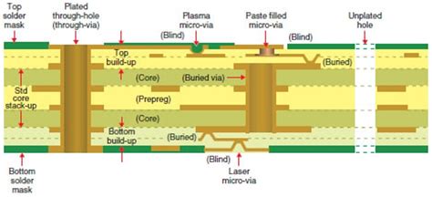
Via usage: Vias are used to connect routing paths between different layers. Minimizing the number of vias can help increase routing density, as vias consume valuable space on the PCB or IC.
-
Trace width and spacing: The width of the routing traces and the spacing between them can also impact routing density. Narrower traces and smaller spacing can allow for more routing paths within a given area, but they also increase the manufacturing complexity and cost.
Comparing Routing Density
The routing density achieved by switchback and serpentine routing can vary depending on the specific design and constraints. In general, serpentine routing can achieve higher routing density compared to switchback routing, as it does not require the additional space needed for the zig-zag pattern.
However, switchback routing can be more advantageous in situations where there are obstacles or constraints that prevent a straight routing path. In such cases, switchback routing can provide more flexibility in navigating around these obstacles, albeit at the cost of increased routing length and potentially lower routing density.
| Routing Technique | Advantages | Disadvantages |
|---|---|---|
| Switchback Routing | – Flexibility in navigating obstacles – Reduced crosstalk – Improved signal integrity |
– Increased routing length – Lower routing density |
| Serpentine Routing | – Delay matching – Impedance control – Space efficiency |
– Increased crosstalk – Limited flexibility |
Best Practices for Maximizing Routing Density
To maximize routing density in PCB and IC designs, designers can follow these best practices:
-
Optimize component placement: Place components strategically to minimize the routing length and maximize the available space for routing.
-
Use multiple routing layers: Increase the number of routing layers to provide more space for routing paths, while considering the manufacturing cost and complexity.
-
Minimize via usage: Reduce the number of vias to conserve space on the PCB or IC, and consider using blind and buried vias when necessary.
-
Adjust trace width and spacing: Use the appropriate trace width and spacing based on the design requirements and manufacturing capabilities to maximize routing density while maintaining signal integrity.
-
Utilize advanced routing techniques: Employ advanced routing techniques, such as differential pair routing and length matching, to optimize signal integrity and timing while maximizing routing density.
Frequently Asked Questions (FAQ)
-
What is the main difference between switchback routing and serpentine routing?
Switchback routing follows a zig-zag pattern, alternating between horizontal and vertical segments, while serpentine routing follows a wavy or sinusoidal pattern. -
Which routing technique is better for maximizing routing density?
Serpentine routing can generally achieve higher routing density compared to switchback routing, as it does not require the additional space needed for the zig-zag pattern. However, the choice between the two techniques depends on various factors, such as the specific design requirements and constraints. -
How does component placement affect routing density?
Component placement can significantly impact routing density. By optimizing the placement of components, designers can minimize the routing length and maximize the available space for routing, leading to higher routing density. -
What is the role of vias in routing density?
Vias are used to connect routing paths between different layers on a PCB or IC. Minimizing the number of vias can help increase routing density, as vias consume valuable space on the board or chip. -
How can designers balance routing density and signal integrity?
Designers can balance routing density and signal integrity by using appropriate trace widths and spacing, employing advanced routing techniques such as differential pair routing and length matching, and optimizing component placement to minimize crosstalk and improve signal quality.
Conclusion
Maximizing routing density is a critical aspect of PCB and IC design, as it enables the integration of more components and functionality into a smaller space. Switchback routing and serpentine routing are two common techniques used to achieve high routing density, each with its own advantages and disadvantages.
While serpentine routing can generally achieve higher routing density compared to switchback routing, the choice between the two techniques depends on various factors, such as the specific design requirements, available space, and desired signal integrity.
By following best practices such as optimizing component placement, using multiple routing layers, minimizing via usage, adjusting trace width and spacing, and utilizing advanced routing techniques, designers can effectively maximize routing density while maintaining signal integrity in their PCB and IC designs.
As technology continues to advance and the demand for more compact and efficient electronic devices grows, the importance of maximizing routing density will only increase. By understanding the differences between switchback and serpentine routing and applying the appropriate techniques based on the specific design requirements, designers can create high-density, high-performance PCBs and ICs that meet the evolving needs of the industry.
No responses yet