Introduction to Rigid-Flex PCB Design in Altium Designer
Rigid-flex PCBs are a combination of rigid and flexible PCBs that offer unique advantages over traditional rigid PCBs. They allow for more compact and lightweight designs, increased reliability, and improved signal integrity. Altium Designer is a powerful PCB design software that provides comprehensive support for rigid-flex PCB design. In this article, we will explore the various features and techniques for designing rigid-flex PCBs in Altium Designer.
What is a Rigid-Flex PCB?
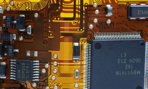
A rigid-flex PCB is a printed circuit board that combines rigid and flexible substrates. The rigid portions of the board provide structural support and house the majority of the components, while the flexible portions allow the board to bend and fold, enabling more compact and three-dimensional packaging. Rigid-flex PCBs are commonly used in applications where space is limited, such as wearable devices, medical equipment, and aerospace systems.
Benefits of Rigid-Flex PCBs
- Space Savings: Rigid-flex PCBs enable more compact packaging by allowing the board to fold and conform to the available space.
- Weight Reduction: By eliminating the need for connectors and cables between rigid boards, rigid-flex PCBs can significantly reduce the overall weight of the system.
- Increased Reliability: Rigid-flex PCBs eliminate the need for connectors, which are often points of failure in traditional multi-board systems.
- Improved Signal Integrity: The elimination of connectors and the use of controlled impedance traces on the flexible portions of the board can improve signal integrity and reduce noise.
Designing Rigid-Flex PCBs in Altium Designer
Setting Up the Layer Stack
The first step in designing a rigid-flex PCB in Altium Designer is to set up the layer stack. The layer stack defines the arrangement of copper layers, dielectric materials, and adhesives that make up the board. In a rigid-flex design, the layer stack will include both rigid and flexible sections.
To set up the layer stack in Altium Designer:
- Open the Layer Stack Manager (Design > Layer Stack Manager).
- Define the rigid and flexible sections of the board by adding dielectric layers and specifying their material properties.
- Assign copper layers to the appropriate sections and specify their thickness and material.
- Define the adhesive layers between the rigid and flexible sections.
Creating the Board Shape
Once the layer stack is defined, the next step is to create the board shape. In a rigid-flex design, the board shape will include both rigid and flexible regions. Altium Designer provides tools for defining the board shape and specifying the boundaries between the rigid and flexible sections.
To create the board shape:
- Open the PCB editor and create a new PCB document.
- Use the Board Shape Primitives to draw the outline of the rigid sections of the board.
- Use the Flexible Region Primitives to draw the outline of the flexible sections of the board.
- Specify the layer stack regions for each section of the board.
Placing Components
When placing components on a rigid-flex PCB, it is important to consider the mechanical requirements of the design. Components should be placed on the rigid sections of the board whenever possible to avoid stress on the flexible sections during bending.
To place components:
- Open the PCB library and select the components to be placed.
- Use the Placement tools to position the components on the rigid sections of the board.
- Use the 3D view to verify that the component placement allows for the desired bending and folding of the flexible sections.
Routing the Board
Routing a rigid-flex PCB requires careful consideration of the mechanical and electrical requirements of the design. The flexible sections of the board should be routed with gentle curves to avoid sharp bends that can cause stress and damage to the copper traces. Controlled impedance traces may be required on the flexible sections to maintain signal integrity.
To route the board:
- Use the Interactive Routing tools to route the traces on the rigid sections of the board.
- Use the Flexible Routing tools to route the traces on the flexible sections of the board, following the contours of the flexible regions.
- Use the Length Tuning tools to adjust the length of the traces for timing and signal integrity.
- Use the 3D view to verify that the routing allows for the desired bending and folding of the flexible sections.
Defining the Bend Areas
In a rigid-flex design, the flexible sections of the board will be bent and folded to achieve the desired packaging. Altium Designer provides tools for defining the bend areas and specifying the bend radius and angle.
To define the bend areas:
- Use the Flexible Bend Area Primitives to draw the bend areas on the flexible sections of the board.
- Specify the bend radius and angle for each bend area.
- Use the 3D view to verify that the bend areas are correctly defined and allow for the desired folding of the board.
Adding Stiffeners and Coverlay
Stiffeners and coverlay are used in rigid-flex designs to provide additional support and protection for the flexible sections of the board. Stiffeners are typically added to the ends of the flexible sections to prevent damage during bending, while coverlay is used to protect the exposed copper traces on the flexible sections.
To add stiffeners and coverlay:
- Use the Stiffener Primitives to draw the stiffener shapes on the flexible sections of the board.
- Specify the stiffener material and thickness.
- Use the Coverlay Primitives to draw the coverlay shapes on the flexible sections of the board.
- Specify the coverlay material and thickness.
Best Practices for Rigid-Flex PCB Design
Use Gradual Bends
When designing the flexible sections of the board, it is important to use gradual bends to avoid stress and damage to the copper traces. Sharp bends can cause the traces to crack or delaminate, leading to reliability issues. A minimum bend radius of 10 times the thickness of the flexible material is recommended.
Avoid Placing Components on Flexible Sections
Placing components on the flexible sections of the board can cause stress and damage during bending. Whenever possible, components should be placed on the rigid sections of the board. If components must be placed on the flexible sections, they should be small, lightweight, and able to withstand the mechanical stress of bending.
Use Strain Relief Features
Strain relief features, such as slots or holes, can be added to the flexible sections of the board to reduce stress and prevent damage during bending. These features allow the flexible material to stretch and compress without putting excessive strain on the copper traces.
Consider the Bend Radius and Angle
When defining the bend areas, it is important to consider the bend radius and angle. A larger bend radius will result in less stress on the copper traces but may require more space. The bend angle should be chosen based on the mechanical requirements of the application and the limitations of the flexible material.
Use Controlled Impedance Traces
Controlled impedance traces may be required on the flexible sections of the board to maintain signal integrity. Altium Designer provides tools for defining and simulating controlled impedance traces, including differential pairs and microstrips.

Conclusion
Rigid-flex PCBs offer unique advantages over traditional rigid PCBs, including space savings, weight reduction, increased reliability, and improved signal integrity. Altium Designer provides comprehensive support for rigid-flex PCB design, with tools for setting up the layer stack, creating the board shape, placing components, routing the board, defining bend areas, and adding stiffeners and coverlay.
By following best practices such as using gradual bends, avoiding placing components on flexible sections, using strain relief features, considering the bend radius and angle, and using controlled impedance traces, designers can create reliable and high-performance rigid-flex PCBs in Altium Designer.
Frequently Asked Questions (FAQ)
- What is the minimum bend radius for a flexible PCB?
-
The minimum bend radius for a flexible PCB depends on the thickness and material of the flexible substrate. A general rule of thumb is to use a minimum bend radius of 10 times the thickness of the flexible material. For example, if the flexible substrate is 0.2 mm thick, the minimum bend radius should be 2 mm.
-
Can I place components on the flexible sections of the board?
-
It is generally recommended to avoid placing components on the flexible sections of the board, as this can cause stress and damage during bending. If components must be placed on the flexible sections, they should be small, lightweight, and able to withstand the mechanical stress of bending.
-
What is the purpose of stiffeners in a rigid-flex PCB?
-
Stiffeners are used in rigid-flex PCBs to provide additional support and protection for the flexible sections of the board. They are typically added to the ends of the flexible sections to prevent damage during bending and to ensure that the flexible sections maintain their shape.
-
How do I define controlled impedance traces in Altium Designer?
-
Altium Designer provides tools for defining and simulating controlled impedance traces, including differential pairs and microstrips. To define controlled impedance traces, you can use the Layer Stack Manager to specify the dielectric material and thickness, and then use the PCB Rules and Constraints Editor to define the trace width and spacing for the desired impedance.
-
What are the benefits of using rigid-flex PCBs?
- Rigid-flex PCBs offer several benefits over traditional rigid PCBs, including:
- Space savings: Rigid-flex PCBs enable more compact packaging by allowing the board to fold and conform to the available space.
- Weight reduction: By eliminating the need for connectors and cables between rigid boards, rigid-flex PCBs can significantly reduce the overall weight of the system.
- Increased reliability: Rigid-flex PCBs eliminate the need for connectors, which are often points of failure in traditional multi-board systems.
- Improved signal integrity: The elimination of connectors and the use of controlled impedance traces on the flexible portions of the board can improve signal integrity and reduce noise.
No responses yet