Introduction to Averatek ASAP
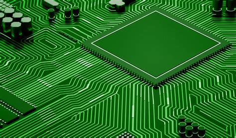
Averatek ASAP (Advanced Subtractive Additive Process) is a groundbreaking technology that enables the creation of high-density printed circuit boards (PCBs) with trace widths and spaces below 25 microns. This innovative process combines the best of both subtractive and additive manufacturing techniques, resulting in PCBs with unparalleled precision, reliability, and performance.
Key Features of Averatek ASAP
- Sub 25 micron trace and space capabilities
- Combines subtractive and additive manufacturing
- High precision and reliability
- Enables miniaturization of electronic devices
- Cost-effective solution for high-density PCBs
How Averatek ASAP Works
The Averatek ASAP process consists of several key steps that enable the creation of ultra-fine traces and spaces on PCBs:
-
Subtractive Etching: The process begins with a standard copper-clad laminate, which undergoes subtractive etching to create a base circuit pattern with trace widths and spaces down to 50 microns.
-
Photoresist Application: A thin layer of photoresist is applied to the etched substrate, covering the base circuit pattern.
-
Laser Direct Imaging: High-precision laser direct imaging is used to expose the photoresist, creating a pattern for the sub 25 micron traces and spaces.
-
Photoresist Development: The exposed photoresist is developed, revealing the ultra-fine trace pattern on the substrate.
-
Additive Plating: The substrate undergoes an additive plating process, depositing copper onto the exposed areas to form the sub 25 micron traces.
-
Photoresist Stripping: The remaining photoresist is stripped away, leaving behind the completed high-density PCB with sub 25 micron traces and spaces.
Averatek ASAP Process Flow
| Step | Description |
|---|---|
| 1 | Subtractive etching of base circuit pattern |
| 2 | Photoresist application |
| 3 | Laser direct imaging of sub 25 micron pattern |
| 4 | Photoresist development |
| 5 | Additive plating of sub 25 micron traces |
| 6 | Photoresist stripping |

Benefits of Sub 25 Micron Traces
The ability to create PCBs with sub 25 micron traces and spaces offers numerous benefits for the electronics industry:
Miniaturization
Sub 25 micron traces enable the design of smaller, more compact electronic devices. This is particularly important in applications such as wearable technology, implantable medical devices, and miniaturized sensors, where space is at a premium.
Increased Functionality
With the ability to pack more traces into a smaller area, designers can incorporate more functionality into their devices without increasing the overall size. This leads to more capable and sophisticated electronic products.
Improved Signal Integrity
Smaller traces and spaces result in shorter signal paths, reducing the potential for signal degradation and interference. This is crucial for high-speed applications, such as 5G communication systems and high-performance computing.
Cost Reduction
By enabling the production of high-density PCBs on standard substrates, Averatek ASAP helps reduce the cost of manufacturing compared to other advanced PCB technologies. This makes sub 25 micron traces more accessible to a wider range of applications and industries.

Applications of Averatek ASAP Technology
The sub 25 micron trace capabilities offered by Averatek ASAP technology find applications in various industries and sectors:
Consumer Electronics
- Smartphones and tablets
- Wearable devices (smartwatches, fitness trackers)
- Virtual and augmented reality headsets
- High-resolution displays
Medical Devices
- Implantable devices (pacemakers, neurostimulators)
- Miniaturized sensors and diagnostic tools
- Wearable health monitoring systems
- Lab-on-a-chip devices
Automotive Electronics
- Advanced driver assistance systems (ADAS)
- In-vehicle infotainment systems
- Miniaturized sensors (pressure, temperature, proximity)
- Electric and hybrid vehicle power electronics
Aerospace and Defense
- Miniaturized satellites (CubeSats)
- Unmanned aerial vehicles (UAVs)
- Missile guidance systems
- Portable communication devices
Industrial Automation
- Miniaturized sensors and actuators
- Embedded control systems
- Wireless sensor networks
- Industrial Internet of Things (IIoT) devices

Case Studies
Case Study 1: Miniaturized Wearable Medical Device
A medical device company utilized Averatek ASAP technology to develop a miniaturized, wearable glucose monitoring system for diabetes patients. The sub 25 micron traces enabled the integration of a continuous glucose sensor, wireless communication module, and battery management system into a compact, watch-sized device. This improved patient comfort and compliance while providing real-time glucose data to healthcare providers.
Case Study 2: High-Density Automotive Radar Module
An automotive electronics manufacturer employed Averatek ASAP to design a high-density radar module for advanced driver assistance systems (ADAS). The sub 25 micron traces allowed for the integration of multiple radar transceivers, signal processing units, and power management components into a single, compact module. This resulted in improved radar performance, reduced system complexity, and lower manufacturing costs compared to traditional PCB technologies.
Comparison with Other PCB Technologies
| Technology | Minimum Trace/Space (μm) | Advantages | Disadvantages |
|---|---|---|---|
| Averatek ASAP | <25 | High density, cost-effective, standard substrates | Limited layer count, requires specialized equipment |
| mSAP | 30-50 | High density, multiple layers | Higher cost, requires specialized materials |
| HDI | 50-100 | Established technology, multiple layers | Limited density, higher cost for finer features |
| Standard PCB | >100 | Low cost, widely available | Limited density, not suitable for miniaturization |
Implementing Averatek ASAP in Your Design
To take advantage of the benefits offered by Averatek ASAP technology, consider the following steps when designing your PCB:
-
Define Requirements: Determine the trace and space requirements for your application, considering factors such as signal integrity, power distribution, and component placement.
-
Choose a PCB Manufacturer: Select a PCB manufacturer that offers Averatek ASAP technology and has experience in producing high-density PCBs.
-
Design for Manufacturability: Work closely with your PCB manufacturer to ensure your design is optimized for the Averatek ASAP process. Consider design rules, layer stackup, and testing requirements.
-
Prototype and Test: Produce prototypes of your design and conduct thorough testing to validate performance, reliability, and manufacturability.
-
Scale Up Production: Once your design is validated, work with your PCB manufacturer to scale up production, taking advantage of the cost and time savings offered by Averatek ASAP technology.
Frequently Asked Questions (FAQ)
1. What is the minimum trace width and space achievable with Averatek ASAP technology?
Averatek ASAP technology enables the creation of traces and spaces below 25 microns, with some designs achieving features as small as 15 microns.
2. Can Averatek ASAP be used with standard PCB substrates?
Yes, one of the key advantages of Averatek ASAP is its compatibility with standard PCB substrates, such as FR-4. This helps reduce costs compared to other advanced PCB technologies that require specialized materials.
3. How does Averatek ASAP compare to other high-density PCB technologies, such as mSAP and HDI?
Averatek ASAP offers finer trace and space capabilities compared to mSAP and HDI, while maintaining a lower cost and compatibility with standard substrates. However, mSAP and HDI technologies may offer advantages in terms of layer count and established manufacturing processes.
4. What are the key applications for sub 25 micron traces enabled by Averatek ASAP?
Sub 25 micron traces find applications in various industries, including consumer electronics, medical devices, automotive electronics, aerospace and defense, and industrial automation. They are particularly beneficial for applications that require miniaturization, increased functionality, and improved signal integrity.
5. How can I get started with designing PCBs using Averatek ASAP technology?
To get started with Averatek ASAP, define your PCB requirements, choose a manufacturer that offers the technology, and work closely with them to optimize your design for manufacturability. Produce prototypes, conduct thorough testing, and then scale up production to take full advantage of the benefits offered by sub 25 micron traces.
Conclusion
Averatek ASAP technology represents a significant advancement in PCB manufacturing, enabling the creation of sub 25 micron traces and spaces. By combining subtractive and additive manufacturing techniques, Averatek ASAP offers a cost-effective solution for producing high-density PCBs on standard substrates.
The ability to create ultra-fine traces and spaces opens up new possibilities for miniaturization, increased functionality, and improved signal integrity in electronic devices. From consumer electronics to medical devices and automotive electronics, sub 25 micron traces find applications in a wide range of industries and sectors.
As the demand for smaller, more capable electronic devices continues to grow, Averatek ASAP technology is poised to play a crucial role in enabling the next generation of PCB designs. By understanding the benefits and applications of sub 25 micron traces, and working closely with experienced PCB manufacturers, designers can unlock the full potential of this innovative technology.

No responses yet