What are Stripline and Microstrip Transmission Lines?
Stripline and microstrip are two common types of planar transmission lines used in printed circuit board (PCB) design to route high-frequency signals. Both consist of a flat conductor separated from a ground plane by a dielectric substrate material. However, they have some key differences in terms of structure, performance characteristics, and PCB Routing guidelines.
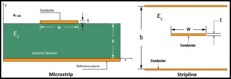
A stripline is a flat conductor sandwiched between two parallel ground planes with a dielectric material in between. The width of the conductor and the thickness and permittivity of the dielectric determine the characteristic impedance of the stripline.
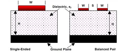
A microstrip line has a single conductor trace on one side of a dielectric substrate with a ground plane on the other side. The width of the trace, the thickness of the substrate, and the permittivity of the dielectric determine its characteristic impedance.
Here is a comparison of the structures of stripline and microstrip:
| Parameter | Stripline | Microstrip |
|---|---|---|
| Conductor geometry | Flat conductor between two ground planes | Flat conductor above a single ground plane |
| Dielectric layers | Conductor surrounded by homogeneous dielectric | Conductor on one side, air on other side of dielectric |
| Fabrication | Requires multiple PCB layers | Can be fabricated on a single PCB layer |
Stripline Characteristics and Benefits
Striplines have several benefits and unique characteristics compared to microstrips:
Shielding and Crosstalk Immunity
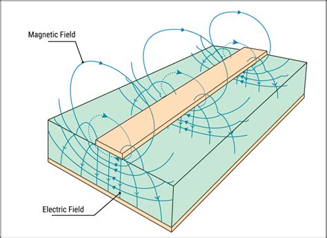
Since the signal conductor in a stripline is sandwiched between two ground planes, it provides excellent shielding against electromagnetic interference (EMI) and reduces crosstalk between adjacent signals. The ground planes act as barriers, confining the electromagnetic fields within the dielectric.
Consistent Impedance
The homogeneous dielectric surrounding the stripline conductor results in a more consistent characteristic impedance along the length of the transmission line. This is because the effective dielectric constant remains constant, as there are no abrupt changes in the dielectric material.
Lower Dispersion
Striplines exhibit lower dispersion than microstrips, meaning that signals of different frequencies propagate at more similar velocities. This is advantageous for high-speed digital signals and broadband applications, as it minimizes signal distortion and maintains signal integrity.
Higher Power Handling
The presence of two ground planes and a homogeneous dielectric allows striplines to handle higher power levels compared to microstrips. The increased heat dissipation and reduced risk of dielectric breakdown make striplines suitable for high-power applications.
Microstrip Characteristics and Benefits
Microstrips also offer several advantages and have distinct characteristics:
Simplicity and Lower Cost
Microstrip transmission lines are simpler to fabricate compared to striplines, as they require only a single conductor layer and a ground plane. This simplicity translates to lower manufacturing costs and easier PCB assembly.
Smaller PCB Footprint
Since microstrips do not require an additional dielectric layer and ground plane, they occupy less space on the PCB. This allows for more compact designs and higher component density, which is particularly important in space-constrained applications.
Easier Access and Probing
The exposed conductor in a microstrip makes it easier to access for probing, testing, and debugging purposes. This accessibility is valuable during the prototyping and testing phases of PCB development.
Compatibility with Surface Mount Components
Microstrips are well-suited for direct integration with surface mount components. The exposed conductor allows for easy soldering and connection to component pads, simplifying the PCB assembly process.

PCB Routing Guidelines for Striplines
When routing striplines on a PCB, consider the following guidelines to ensure optimal performance and signal integrity:
Maintain Constant Impedance
To maintain a constant characteristic impedance along the stripline, ensure that the conductor width, dielectric thickness, and dielectric constant remain consistent throughout the route. Avoid abrupt changes in geometry or materials that can cause impedance discontinuities.
Provide Adequate Spacing
Maintain sufficient spacing between adjacent striplines to minimize crosstalk and electromagnetic coupling. The spacing should be based on the signal frequencies, dielectric properties, and the required level of isolation. Consult PCB design guidelines and use simulation tools to determine appropriate spacing.
Minimize Discontinuities
Avoid abrupt changes in the stripline geometry, such as sharp bends or transitions to different layer stackups. Discontinuities can cause reflections, signal distortion, and impedance mismatches. Use smooth bends and gradual transitions to maintain signal integrity.
Consider Grounding and Shielding
Ensure proper grounding of the stripline by connecting the ground planes to a low-impedance ground reference. Provide sufficient vias to create a robust ground connection. If additional shielding is required, consider using guard traces or additional ground layers to isolate sensitive signals.
Optimize Via Transitions
When transitioning striplines between PCB layers, use vias designed for high-frequency signals. Minimize the via length and diameter to reduce parasitic inductance and capacitance. Consider using microvias or buried vias for improved signal integrity and reduced discontinuities.
PCB Routing Guidelines for Microstrips
When routing microstrips on a PCB, follow these guidelines to ensure proper performance and signal quality:
Maintain Characteristic Impedance
Control the microstrip impedance by adjusting the trace width, substrate thickness, and dielectric constant. Use PCB design tools and calculators to determine the appropriate trace dimensions for the desired impedance. Maintain a consistent trace width along the entire route to avoid impedance mismatches.
Provide Adequate Clearance
Ensure sufficient clearance between the microstrip and adjacent traces or components to minimize electromagnetic coupling and crosstalk. Follow the PCB manufacturer’s design rules and guidelines for minimum spacing requirements based on the signal frequencies and PCB fabrication capabilities.
Minimize Trace Length
Keep microstrip traces as short as possible to reduce signal attenuation, delay, and susceptibility to external noise. Minimize the distance between the source and destination components, and avoid unnecessary routing detours. Shorter traces also help in maintaining signal integrity and reducing reflections.
Consider Trace Thickness
Choose an appropriate trace thickness for the microstrip based on the current carrying requirements and the desired characteristic impedance. Thicker traces have lower resistance and can handle higher currents, but they also have higher capacitance and may require adjustments to the trace width to maintain the target impedance.
Minimize Discontinuities
Similar to striplines, avoid abrupt changes in the microstrip geometry. Use smooth bends and gradual transitions to minimize reflections and impedance discontinuities. If necessary, use mitered bends or chamfered corners to reduce the effects of discontinuities.
Provide Proper Grounding
Ensure a solid and low-impedance ground reference for the microstrip by providing sufficient ground plane coverage. Use ground vias to connect the ground plane to other ground layers or components. Proper grounding helps in reducing electromagnetic interference and maintaining signal integrity.
Frequently Asked Questions (FAQ)
-
Q: When should I choose stripline over microstrip for my PCB design?
A: Stripline is preferred when you require better shielding, lower crosstalk, and higher power handling capability. It is suitable for designs with high signal densities and strict EMI requirements. Microstrip is a good choice when simplicity, lower cost, and smaller PCB footprint are priorities. -
Q: Can I mix striplines and microstrips on the same PCB?
A: Yes, it is possible to use both striplines and microstrips on the same PCB. However, ensure proper transitions between the two transmission line types to maintain signal integrity. Use appropriate layer transitions and impedance matching techniques to minimize reflections and discontinuities. -
Q: How do I calculate the characteristic impedance of striplines and microstrips?
A: The characteristic impedance of striplines and microstrips depends on factors such as the conductor width, dielectric thickness, and dielectric constant. You can use online calculators, PCB design software, or mathematical formulas to determine the impedance. Consult the respective tools or reference materials for accurate calculations. -
Q: What is the impact of dielectric material on stripline and microstrip performance?
A: The dielectric material affects the propagation velocity, impedance, and loss characteristics of striplines and microstrips. Materials with lower dielectric constants result in faster signal propagation and lower capacitance. Higher-quality dielectrics with lower loss tangents minimize signal attenuation and maintain signal integrity. -
Q: How do I handle high-speed signals when routing striplines and microstrips?
A: When dealing with high-speed signals, pay attention to impedance matching, signal rise times, and propagation delays. Ensure proper termination to prevent reflections and ringing. Use simulation tools to analyze signal integrity and optimize the PCB layout. Follow high-speed design guidelines for trace routing, spacing, and layer stackup to minimize signal distortion and crosstalk.
By understanding the characteristics, benefits, and routing guidelines for striplines and microstrips, PCB designers can make informed decisions when selecting the appropriate transmission line for their specific application. Proper design and routing techniques ensure optimal signal integrity, EMI control, and overall PCB performance.
No responses yet