Introduction to PCB Ground Planes and Grounding Techniques
Proper grounding is essential for the optimal performance, signal integrity, and electromagnetic compatibility of printed circuit boards (PCBs). In PCB layout, ground planes serve as a reference point for signals and help to minimize noise, crosstalk, and electromagnetic interference (EMI). This article will explore the different types of ground planes, their roles in PCB design, and best practices for implementing them effectively.
Types of Ground Planes in PCB Layout
There are three main types of ground planes used in PCB layout:
- Digital Ground Plane
- Analog Ground Plane
- Earth Ground Plane
Each type of ground plane serves a specific purpose and requires careful consideration during the PCB design process.
Digital Ground Plane
The digital ground plane is used as a reference for digital signals and components such as microprocessors, digital ICs, and digital communication interfaces. It provides a low-impedance return path for high-frequency digital signals, minimizing noise and ensuring signal integrity.
Key characteristics of a digital ground plane include:
- Large, uninterrupted copper pour
- Connected to digital components and their ground pins
- Separated from analog and earth ground planes
Analog Ground Plane
The analog ground plane is used as a reference for analog signals and components such as operational amplifiers, analog-to-digital converters (ADCs), and analog sensors. It helps to isolate sensitive analog circuits from digital noise and interference.
Key characteristics of an analog ground plane include:
- Separate from digital ground plane to avoid noise coupling
- Connected to analog components and their ground pins
- May be further divided into multiple analog ground domains for different analog subcircuits
Earth Ground Plane
The earth ground plane, also known as chassis ground or safety ground, is connected to the metal chassis or enclosure of the device. Its primary purpose is to provide a safe discharge path for electromagnetic interference (EMI) and electrostatic discharge (ESD), protecting users from electrical hazards.
Key characteristics of an earth ground plane include:
- Connected to the metal chassis or enclosure
- Linked to the digital and analog ground planes through a single, low-impedance connection
- Helps to shield the PCB from external EMI
Best Practices for Implementing Ground Planes in PCB Layout
To ensure optimal performance and minimize issues related to noise, crosstalk, and EMI, follow these best practices when implementing ground planes in your PCB layout:
1. Use Solid Ground Planes
Whenever possible, use solid, uninterrupted ground planes rather than gridded or hatched patterns. Solid ground planes provide the lowest impedance and best shielding against EMI.
2. Separate Digital and Analog Ground Planes
Keep digital and analog ground planes separate to minimize noise coupling between digital and analog circuits. Connect the two ground planes at a single, low-impedance point, such as near the power supply or at the ADC/DAC interface.
3. Minimize Ground Plane Cuts and Slots
Avoid cutting or slotting the ground planes unnecessarily, as this can disrupt the flow of return currents and create impedance discontinuities. If cuts or slots are necessary, keep them as small as possible and perpendicular to the direction of signal traces.
4. Use Ground Stitching Vias
When using multiple ground planes or layers, connect them together with ground stitching vias. This helps to maintain a low-impedance connection between the planes and improves EMI shielding. Place ground stitching vias at regular intervals, especially along the edges of the PCB.
5. Keep Ground Connections Short
Minimize the length of ground connections between components and the ground plane. Long ground traces can introduce inductance and create impedance mismatches, leading to signal integrity issues and EMI.
6. Use Ground Pours on Signal Layers
In addition to dedicated ground planes, use ground pours on signal layers to provide a low-impedance return path for signals. This helps to reduce crosstalk and improve signal integrity. Ensure that ground pours are connected to the appropriate ground plane using vias.
7. Consider Split Ground Planes for Mixed-Signal Designs
In mixed-signal designs with both digital and analog circuits, consider using a split ground plane to further isolate the two domains. A split ground plane has separate digital and analog sections that are connected at a single point, typically near the ADC/DAC interface or power supply.
Grounding Techniques for Specific PCB Applications
Different PCB applications may require specific grounding techniques to ensure optimal performance and electromagnetic compatibility. Here are some grounding considerations for common PCB applications:
High-Speed Digital Designs
In high-speed digital designs, proper grounding is critical for maintaining signal integrity and minimizing EMI. Follow these guidelines:
- Use a continuous, low-impedance digital ground plane
- Minimize ground plane cuts and slots
- Use ground stitching vias to connect ground planes on different layers
- Keep ground connections short and direct
- Use ground pours on signal layers to provide a low-impedance return path
RF and Wireless Designs
RF and wireless PCBs require careful grounding to minimize signal loss, ensure proper impedance matching, and reduce EMI. Consider these techniques:
- Use a solid, uninterrupted ground plane for RF signals
- Keep RF ground connections short and direct
- Use via fencing around RF components to minimize coupling with other circuits
- Isolate RF ground from digital and analog ground planes
- Use RF-specific components, such as RF chokes and capacitors, to maintain signal integrity
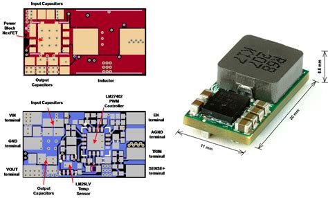
Power Electronics Designs
Power electronics PCBs, such as those used in motor drives and power supplies, require special attention to grounding to ensure safety and minimize EMI. Follow these practices:
- Use a solid, low-impedance ground plane for power components
- Separate power ground from digital and analog ground planes
- Use star grounding techniques to minimize ground loops
- Employ proper isolation techniques, such as optocouplers or transformers, between power and control circuits
- Follow safety standards and guidelines for power electronics grounding

Advanced Grounding Techniques for Noise Reduction and EMI Mitigation
In addition to basic grounding practices, advanced techniques can be used to further reduce noise, mitigate EMI, and improve overall PCB performance. Some of these techniques include:
Ground Plane Segmentation
Ground plane segmentation involves dividing the ground plane into separate regions for different circuit functions or frequency domains. This technique helps to isolate noisy circuits from sensitive ones and can reduce crosstalk and EMI.
To implement ground plane segmentation:
- Identify circuit blocks or functional areas that generate or are sensitive to noise
- Create separate ground plane regions for each block or area
- Connect the segments using a single, low-impedance connection, such as a ferrite bead or a small inductor
- Use ground stitching vias to maintain a low-impedance connection between the segments
Moating and Guarding
Moating and guarding are techniques used to isolate sensitive analog circuits from digital noise and interference. A moat is a small, continuous gap in the ground plane that surrounds a sensitive analog component or circuit. A guard is a conductive trace or ring that surrounds the moat and is connected to the analog ground plane.
To implement moating and guarding:
- Identify sensitive analog components or circuits
- Create a moat by removing copper from the ground plane around the sensitive area
- Place a guard trace or ring around the moat, connecting it to the analog ground plane
- Ensure that the guard trace is not connected to the digital ground plane or any other noisy circuits
Shielding and Filtering
Shielding and filtering techniques can be used to minimize EMI and reduce the impact of external noise sources on the PCB.
-
Shielding involves enclosing sensitive circuits or components in a conductive enclosure, such as a metal can or a shielded compartment on the PCB. This helps to block external EMI and contain internal EMI generated by the circuit.
-
Filtering involves using passive components, such as capacitors, inductors, and ferrites, to attenuate noise and high-frequency interference. Common filtering techniques include decoupling capacitors, ferrite beads, and LC filters.
To implement shielding and filtering:
- Identify circuits or components that are sensitive to EMI or generate significant noise
- Design a conductive enclosure or compartment around the sensitive area, connected to the ground plane
- Use filtering components, such as decoupling capacitors and ferrite beads, near noise sources and sensitive components
- Follow best practices for component placement and routing to maximize the effectiveness of shielding and filtering
FAQ
1. What is the difference between digital, analog, and earth ground planes in PCB layout?
Digital ground planes are used as a reference for digital signals and components, analog ground planes are used for analog signals and components, and earth ground planes are connected to the metal chassis or enclosure for safety and EMI protection.
2. Why is it important to separate digital and analog ground planes?
Separating digital and analog ground planes helps to minimize noise coupling between digital and analog circuits, ensuring signal integrity and reducing interference.
3. How can I minimize noise and EMI in my PCB layout?
To minimize noise and EMI, use solid ground planes, separate digital and analog grounds, minimize ground plane cuts and slots, use ground stitching vias, keep ground connections short, and employ advanced techniques like ground plane segmentation, moating, guarding, shielding, and filtering.
4. What is the purpose of ground stitching vias?
Ground stitching vias are used to connect ground planes on different layers of the PCB, maintaining a low-impedance connection between the planes and improving EMI shielding.
5. When should I consider using a split ground plane in my PCB design?
Split ground planes are useful in mixed-signal designs with both digital and analog circuits. They help to isolate the digital and analog domains, minimizing noise coupling and ensuring signal integrity.
Conclusion
Proper grounding is essential for the performance, signal integrity, and electromagnetic compatibility of PCBs. By understanding the different types of ground planes, following best practices for their implementation, and employing advanced techniques for noise reduction and EMI mitigation, designers can create PCBs that are reliable, robust, and meet the requirements of their specific applications. Always consider the unique characteristics of your design, the operating environment, and the relevant standards and guidelines when planning your PCB layout and grounding strategy.
| Ground Plane Type | Purpose | Key Characteristics |
|---|---|---|
| Digital Ground | Reference for digital signals and components | Large copper pour, connected to digital components |
| Analog Ground | Reference for analog signals and components | Separate from digital ground, divided into subdomains |
| Earth Ground | Safety and EMI protection, chassis connection | Connected to chassis, linked to digital/analog grounds |
Remember, a well-designed grounding system is the foundation for a successful PCB. By paying close attention to grounding during the layout process, you can minimize issues, optimize performance, and create a product that meets or exceeds expectations.
No responses yet