Introduction to PCB Panel Size
Printed Circuit Boards (PCBs) are essential components in modern electronic devices. They provide a platform for mounting and interconnecting electronic components, enabling the creation of complex circuits. When it comes to manufacturing PCBs, one crucial aspect to consider is the panel size. PCB panel size refers to the dimensions of the larger board from which individual PCBs are cut out. Understanding standard PCB panel sizes is essential for optimizing the manufacturing process, minimizing costs, and ensuring compatibility with assembly equipment.
In this comprehensive article, we will delve into the world of standard PCB panel sizes. We’ll explore the common panel sizes used in the industry, factors influencing panel size selection, and the benefits of utilizing standard sizes. Additionally, we’ll discuss design considerations, manufacturing processes, and frequently asked questions related to PCB panel sizes.
Common PCB Panel Sizes
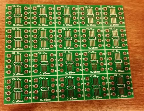
There are several standard PCB panel sizes commonly used in the electronics industry. These sizes have been established to streamline the manufacturing process and ensure compatibility with various equipment and processes. Let’s take a look at some of the most common PCB panel sizes:
1. 18″ x 24″ (457mm x 610mm)
The 18″ x 24″ panel size is one of the most widely used in the PCB industry. It offers a good balance between panel utilization and manufacturing efficiency. This size is suitable for a wide range of PCB Designs and is compatible with most manufacturing equipment.
2. 21″ x 24″ (533mm x 610mm)
The 21″ x 24″ panel size is another popular choice, particularly for larger PCB designs. It provides more space for accommodating complex layouts and higher component densities. This size is commonly used in the production of multi-layer PCBs and high-density interconnect (HDI) boards.
3. 16″ x 18″ (406mm x 457mm)
The 16″ x 18″ panel size is often used for smaller PCB designs or when there are specific manufacturing constraints. It is a good choice for projects with lower production volumes or when cost optimization is a priority.
4. 12″ x 18″ (305mm x 457mm)
The 12″ x 18″ panel size is suitable for smaller PCB designs and is often used in prototyping or low-volume production runs. It offers a cost-effective solution for projects with limited space requirements.
Here’s a table summarizing the common PCB panel sizes:
| Panel Size (inches) | Panel Size (millimeters) |
|---|---|
| 18″ x 24″ | 457mm x 610mm |
| 21″ x 24″ | 533mm x 610mm |
| 16″ x 18″ | 406mm x 457mm |
| 12″ x 18″ | 305mm x 457mm |
Factors Influencing Panel Size Selection
When selecting a PCB panel size, several factors need to be considered to ensure optimal manufacturing results. These factors include:
1. PCB Design Complexity
The complexity of the PCB design plays a significant role in determining the appropriate panel size. More complex designs with higher component densities may require larger panel sizes to accommodate all the necessary features and routing.
2. Manufacturing Equipment Compatibility
It’s crucial to choose a panel size that is compatible with the manufacturing equipment used by the PCB fabricator. Different equipment may have specific size limitations or requirements, so it’s essential to consult with the manufacturer to ensure compatibility.
3. Production Volume
The production volume of the PCB project can also influence the choice of panel size. For high-volume production runs, larger panel sizes are often preferred to maximize efficiency and reduce manufacturing costs. Smaller panel sizes may be more suitable for low-volume or prototype runs.
4. Cost Optimization
Panel size selection can have a significant impact on the overall manufacturing costs. Larger panel sizes allow for more efficient utilization of materials and can reduce the cost per PCB. However, it’s important to strike a balance between panel size and design requirements to avoid unnecessary expenses.

Benefits of Using Standard PCB Panel Sizes
Using standard PCB panel sizes offers several advantages in terms of manufacturing efficiency, cost savings, and reliability. Let’s explore some of the key benefits:
1. Streamlined Manufacturing Process
Standard panel sizes are designed to be compatible with common manufacturing equipment and processes. By utilizing standard sizes, PCB fabricators can optimize their production lines, reducing setup times and minimizing the need for custom tooling. This streamlined approach leads to faster turnaround times and improved overall efficiency.
2. Cost Savings
Using standard panel sizes can result in significant cost savings compared to custom panel sizes. Standard sizes allow for better material utilization, reducing waste and optimizing the use of available space on the panel. Additionally, standard sizes often have pre-established tooling and processes, eliminating the need for costly custom setups.
3. Improved Reliability
Standard panel sizes have been extensively tested and proven in the industry. They have undergone rigorous quality control measures and have a track record of reliable performance. By adhering to standard sizes, manufacturers can ensure consistent results and minimize the risk of manufacturing defects or compatibility issues.
4. Easier Sourcing and Compatibility
Standard panel sizes are widely available from PCB fabricators and suppliers worldwide. This widespread availability makes it easier to source materials and find compatible manufacturing partners. It also ensures that the PCBs can be easily integrated into various electronic devices and systems without the need for custom adaptations.
Design Considerations for PCB Panel Size
When designing PCBs, it’s important to keep panel size considerations in mind to ensure optimal manufacturing results. Here are some key design considerations:
1. Board Outline and Dimensions
The dimensions of the individual PCBs should be carefully planned to maximize the utilization of the panel space. Designers should consider the placement of components, routing, and any required clearances to ensure that the PCBs fit efficiently within the chosen panel size.
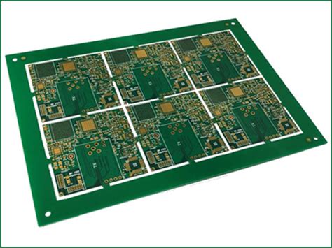
2. Panelization Techniques
Panelization techniques involve arranging multiple PCBs on a single panel to optimize manufacturing efficiency. Common panelization techniques include tab routing, scoring, and mouse bites. Designers should work closely with the PCB fabricator to determine the most suitable panelization method based on the specific design requirements and manufacturing capabilities.
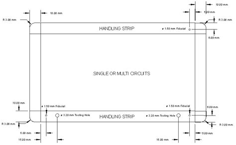
3. Fiducial Marks and Tooling Holes
Fiducial marks and tooling holes are important features that aid in the alignment and registration of the PCBs during the manufacturing process. Designers should include appropriate fiducial marks and tooling holes on the panel to ensure accurate placement and cutting of the individual PCBs.
4. Design for Manufacturing (DFM)
Designing PCBs with manufacturability in mind is crucial for successful production. Designers should adhere to DFM Guidelines, such as maintaining proper trace widths, spacing, and hole sizes, to ensure compatibility with the chosen manufacturing processes and panel sizes.
Manufacturing Process and Panel Size
The manufacturing process for PCBs involves several steps, and panel size plays a role in each stage. Let’s take a closer look at how panel size impacts the manufacturing process:
1. Material Selection
The choice of PCB material, such as FR-4 or high-frequency laminates, should be compatible with the selected panel size. Different materials may have specific size limitations or requirements, so it’s important to consult with the PCB fabricator to ensure compatibility.
2. Photolithography and Etching
During the photolithography and etching process, the PCB design is transferred onto the copper layers of the panel. The panel size determines the number of PCBs that can be accommodated on a single panel, affecting the efficiency and cost of the process.
3. Drilling and Plating
The drilling and plating processes involve creating holes for component mounting and interconnections. The panel size influences the drilling and plating equipment used, as well as the number of panels that can be processed simultaneously.
4. Solder Mask and Silkscreen Application
Solder mask and silkscreen layers are applied to the PCB panel to protect the copper traces and provide component identification. The panel size determines the number of PCBs that can be accommodated in a single application, impacting the efficiency and cost of the process.
5. Cutting and Singulation
After the manufacturing processes are complete, the individual PCBs are cut out from the panel using methods such as routing or punching. The panel size dictates the number of PCBs that can be cut from a single panel and affects the efficiency of the cutting process.
Frequently Asked Questions (FAQ)
-
What is the most commonly used PCB panel size?
The most commonly used PCB panel size is 18″ x 24″ (457mm x 610mm). This size offers a good balance between panel utilization and manufacturing efficiency, making it suitable for a wide range of PCB designs. -
Can I use custom panel sizes for my PCB project?
While custom panel sizes are possible, it’s generally recommended to use standard panel sizes whenever feasible. Standard sizes offer numerous benefits, including compatibility with manufacturing equipment, cost savings, and improved reliability. Custom sizes may require additional tooling and setup, leading to higher costs and longer lead times. -
How does panel size affect the cost of PCB manufacturing?
Panel size can have a significant impact on the cost of PCB manufacturing. Larger panel sizes allow for more efficient utilization of materials and can reduce the cost per PCB. However, it’s important to strike a balance between panel size and design requirements to avoid unnecessary expenses. Using standard panel sizes can also help optimize costs by leveraging established manufacturing processes and tooling. -
What factors should I consider when selecting a PCB panel size?
When selecting a PCB panel size, consider factors such as PCB design complexity, manufacturing equipment compatibility, production volume, and cost optimization. Evaluate the specific requirements of your project and consult with your PCB fabricator to determine the most suitable panel size that aligns with your design goals and manufacturing capabilities. -
Can I mix different PCB designs on the same panel?
Yes, it is possible to mix different PCB designs on the same panel, a practice known as panel sharing or multi-project panelization. This approach can be cost-effective for small-batch production or when multiple designs share similar specifications. However, it’s important to ensure that the designs are compatible in terms of material, thickness, and manufacturing requirements to avoid any issues during the production process.
Conclusion
Understanding standard PCB panel sizes is crucial for anyone involved in the design and manufacturing of printed circuit boards. By utilizing standard panel sizes, you can optimize the manufacturing process, reduce costs, and ensure compatibility with industry-standard equipment and processes.
When selecting a PCB panel size, consider factors such as design complexity, manufacturing equipment compatibility, production volume, and cost optimization. Work closely with your PCB fabricator to determine the most suitable panel size for your specific project requirements.
By adhering to standard panel sizes and following best practices in PCB design, you can streamline the manufacturing process, improve reliability, and achieve successful outcomes for your electronic projects.
Remember, the choice of PCB panel size is not just a technical decision; it also has significant implications for cost, efficiency, and overall project success. By understanding the importance of standard panel sizes and making informed decisions, you can navigate the world of PCB manufacturing with confidence and achieve the best possible results for your electronic devices.
No responses yet