Understanding the Importance of PCB Stackup
When designing a printed circuit board (PCB), one of the most critical aspects to consider is the PCB stackup. The stackup refers to the arrangement of copper layers, insulating layers, and other materials that make up the PCB. The choice of stackup can significantly impact the performance, reliability, and manufacturability of the final product. In this article, we will explore the standard board thicknesses and how they relate to your layer stack.
What is a PCB Stackup?
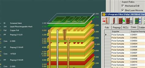
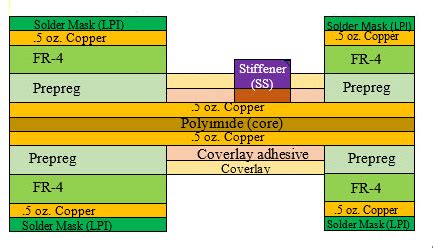
A PCB stackup is a cross-sectional view of the layers that make up a printed circuit board. It shows the arrangement of conductive copper layers, insulating dielectric layers, and other materials such as solder mask and silkscreen. The stackup also specifies the thickness of each layer and the overall thickness of the board.
Why is PCB Stackup Important?
The PCB stackup is essential for several reasons:
-
Signal Integrity: The arrangement of layers can affect the signal integrity of the PCB. For example, placing signal layers close to power or ground planes can help reduce noise and improve signal quality.
-
Impedance Control: The stackup can be designed to achieve specific impedance values for controlled impedance traces, which is crucial for high-speed designs.
-
Manufacturability: The choice of stackup can impact the manufacturability of the PCB. Some stackups may be more challenging to fabricate, leading to higher costs or longer lead times.
-
Reliability: A well-designed stackup can help improve the reliability of the PCB by minimizing the risk of signal integrity issues, thermal problems, or mechanical stress.
Standard Board Thicknesses
PCBs come in various thicknesses, depending on the application and design requirements. The most common board thicknesses are:
| Thickness (mm) | Thickness (mils) | Typical Applications |
|---|---|---|
| 0.4 | 15.75 | Ultra-thin, flexible PCBs |
| 0.6 | 23.62 | Thin, flexible PCBs |
| 0.8 | 31.50 | Thin, rigid PCBs |
| 1.0 | 39.37 | Rigid PCBs |
| 1.2 | 47.24 | Rigid PCBs |
| 1.6 | 62.99 | Thick, rigid PCBs |
| 2.0 | 78.74 | Very thick, rigid PCBs |
The choice of board thickness depends on several factors, such as:
- The number of layers required
- The mechanical strength and rigidity needed
- The space constraints of the final product
- The thermal management requirements
- The cost and availability of materials
How Board Thickness Affects Layer Stack
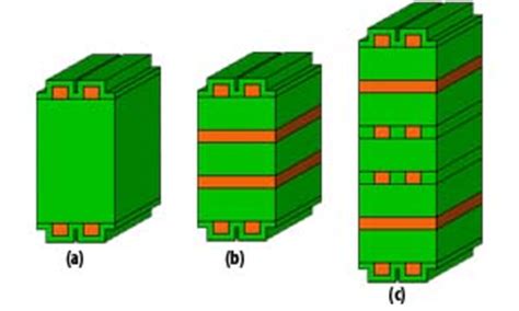
The board thickness directly influences the number of layers that can be accommodated in the PCB stackup. As the board thickness increases, more layers can be added to the stackup. However, adding layers also increases the complexity and cost of the PCB.
Here are some typical layer stacks for different board thicknesses:
0.8mm (4-layer PCB)
| Layer | Material | Thickness (mm) |
|---|---|---|
| Top Copper | Copper | 0.035 |
| Core | FR-4 | 0.710 |
| Bottom Copper | Copper | 0.035 |
| Solder Mask | Ink | 0.010 |
1.6mm (6-layer PCB)
| Layer | Material | Thickness (mm) |
|---|---|---|
| Top Copper | Copper | 0.035 |
| Prepreg | FR-4 | 0.180 |
| Inner Layer 1 | Copper | 0.035 |
| Core | FR-4 | 1.065 |
| Inner Layer 2 | Copper | 0.035 |
| Prepreg | FR-4 | 0.180 |
| Bottom Copper | Copper | 0.035 |
| Solder Mask | Ink | 0.015 |
2.0mm (8-layer PCB)
| Layer | Material | Thickness (mm) |
|---|---|---|
| Top Copper | Copper | 0.035 |
| Prepreg | FR-4 | 0.180 |
| Inner Layer 1 | Copper | 0.035 |
| Core | FR-4 | 0.710 |
| Inner Layer 2 | Copper | 0.035 |
| Core | FR-4 | 0.710 |
| Inner Layer 3 | Copper | 0.035 |
| Prepreg | FR-4 | 0.180 |
| Bottom Copper | Copper | 0.035 |
| Solder Mask | Ink | 0.020 |
As you can see, thicker boards allow for more layers and more complex stackups. However, it’s essential to strike a balance between the number of layers and the overall thickness to ensure the PCB meets the design requirements while remaining cost-effective and manufacturable.
Designing Your Layer Stack
When designing your PCB layer stack, there are several factors to consider:
Signal Integrity
Signal integrity is crucial for ensuring the proper functioning of the PCB. To maintain signal integrity, consider the following:
- Place signal layers close to power or ground planes to minimize noise and crosstalk.
- Use proper grounding techniques, such as ground planes and stitching vias, to provide a low-impedance return path for signals.
- Route high-speed signals on inner layers to minimize the impact of external noise.
Impedance Control
For high-speed designs, controlling the impedance of traces is essential to maintain signal integrity and minimize reflections. To achieve impedance control:
- Choose the appropriate dielectric material and thickness for the desired impedance.
- Adjust the trace width and spacing to achieve the target impedance.
- Use a stackup calculator or simulation tool to optimize the impedance of the traces.
Thermal Management
Proper thermal management is essential to ensure the reliability and longevity of the PCB. To manage heat dissipation:
- Use thicker copper layers for power and ground planes to improve heat spreading.
- Place thermal vias near high-power components to conduct heat to the opposite side of the board.
- Consider using metal core PCBs or other thermal management techniques for high-power applications.
Manufacturability
Designing a PCB stackup that is easy to manufacture can help reduce costs and lead times. To improve manufacturability:
- Follow the manufacturer’s design guidelines for minimum trace width, spacing, and hole size.
- Avoid using uncommon materials or thicknesses that may be difficult to source or process.
- Consider the aspect ratio of vias and the drilling capabilities of the manufacturer.

Frequently Asked Questions (FAQ)
-
What is the most common PCB thickness?
The most common PCB thickness is 1.6mm (62.99 mils). This thickness provides a good balance between mechanical strength, layer count, and cost. -
Can I use a thinner board to reduce costs?
While using a thinner board can reduce material costs, it may not always be the best choice. Thinner boards may be more prone to warping, have limited layer counts, and be more challenging to manufacture. It’s essential to consider the overall design requirements and consult with your manufacturer before choosing a thinner board. -
How many layers can I have in my PCB stackup?
The number of layers in a PCB stackup depends on the board thickness and the design requirements. Most PCBs have between 2 and 12 layers, but some high-density designs can have up to 50 layers or more. However, as the layer count increases, so does the complexity and cost of the PCB. -
What is the minimum board thickness for controlled impedance traces?
The minimum board thickness for controlled impedance traces depends on the dielectric material and the target impedance. In general, a board thickness of 0.8mm or greater is recommended for controlled impedance designs. However, it’s essential to consult with your manufacturer and use simulation tools to determine the optimal stackup for your specific design. -
Can I mix different board thicknesses in the same PCB?
Yes, it is possible to mix different board thicknesses in the same PCB using a technique called “stepped” or “sculpted” routing. This involves varying the thickness of the PCB in specific areas to accommodate components or connectors with different height requirements. However, stepped routing can add complexity and cost to the manufacturing process, so it should be used judiciously.
Conclusion
Choosing the right board thickness and layer stack is critical for ensuring the performance, reliability, and manufacturability of your PCB. By understanding the standard board thicknesses and how they relate to your layer stack, you can make informed decisions when designing your PCB.
When designing your layer stack, consider factors such as signal integrity, impedance control, thermal management, and manufacturability. Use simulation tools and consult with your manufacturer to optimize your stackup for your specific design requirements.
By following best practices and carefully considering your layer stack, you can create PCBs that meet your performance goals while remaining cost-effective and easy to manufacture.
No responses yet