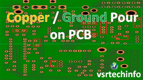
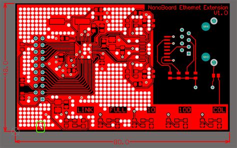
What are PCB Plane Pours?
PCB (Printed Circuit Board) plane pours are large areas of copper that are used to provide a low-impedance connection between components on a PCB. These plane pours are typically used for power and ground connections, as they can provide a much lower impedance than thin traces. The plane pours are created by filling in the unused areas of the PCB with copper, which is then connected to the appropriate components.
Benefits of Using PCB Plane Pours
There are several benefits to using PCB plane pours in your designs:
- Lower Impedance: Plane pours provide a much lower impedance connection than thin traces, which can help to reduce noise and improve signal integrity.
- Better Heat Dissipation: The large area of copper in a plane pour can help to dissipate heat more effectively than thin traces, which can help to improve the reliability of your design.
- Improved EMI Performance: Plane pours can help to reduce electromagnetic interference (EMI) by providing a low-impedance return path for high-frequency signals.
Limitations of PCB Plane Pours
While PCB plane pours can provide many benefits, there are also some limitations to consider:
- Increased Manufacturing Cost: Adding plane pours to your PCB design can increase the manufacturing cost, as it requires additional copper and processing steps.
- Limited Routing Options: Plane pours can limit the available routing options on your PCB, as they take up space that could otherwise be used for traces.
- Potential for Shorts: If not carefully managed, plane pours can create shorts between components or traces on your PCB.
What are Split PCB Plane Pours?
Split PCB plane pours are a technique used to create partial, carefully managed connections between different sections of a plane pour. This technique involves creating a gap or split in the plane pour to separate different sections of the pour. The split can be created using a variety of methods, including:
- Using a PCB design tool to create a gap in the plane pour
- Manually cutting the plane pour during the PCB fabrication process
- Using a milling machine or laser cutter to remove sections of the plane pour
Benefits of Using Split PCB Plane Pours
There are several benefits to using split PCB plane pours in your designs:
- Improved Signal Integrity: By carefully managing the connections between different sections of the plane pour, you can improve the signal integrity of your design. This is particularly important for high-speed designs where signal integrity is critical.
- Reduced Crosstalk: Split plane pours can help to reduce crosstalk between different signals on your PCB by providing separate return paths for each signal.
- Better EMI Performance: By carefully managing the connections between different sections of the plane pour, you can improve the EMI performance of your design.
Limitations of Split PCB Plane Pours
While split PCB plane pours can provide many benefits, there are also some limitations to consider:
- Increased Design Complexity: Creating split plane pours requires careful planning and design, which can increase the complexity of your PCB layout.
- Limited Routing Options: Split plane pours can limit the available routing options on your PCB, as they take up space that could otherwise be used for traces.
- Potential for Shorts: If not carefully managed, split plane pours can create shorts between different sections of the plane pour or between the plane pour and other components on your PCB.
Techniques for Managing Split PCB Plane Pours
There are several techniques that can be used to effectively manage split PCB plane pours in your designs:
1. Use a Ground Plane
One of the most effective techniques for managing split PCB plane pours is to use a dedicated ground plane. By placing a solid ground plane on a separate layer of your PCB, you can provide a low-impedance return path for all of your signals. This can help to improve signal integrity, reduce crosstalk, and improve EMI performance.
When using a ground plane, it’s important to ensure that all of your components are properly connected to the ground plane. This can be accomplished using vias or through-hole connections.
2. Use Stitching Capacitors
Stitching capacitors are small capacitors that are used to provide a low-impedance connection between different sections of a split plane pour. These capacitors are typically placed at regular intervals along the split, and help to ensure that the different sections of the plane pour are properly connected.
When using stitching capacitors, it’s important to choose the appropriate size and spacing for your design. The size of the capacitor will depend on the frequency of the signals in your design, while the spacing will depend on the size of the split and the desired impedance of the connection.
3. Use Stitching Vias
Stitching vias are small vias that are used to provide a low-impedance connection between different sections of a split plane pour. These vias are typically placed at regular intervals along the split, and help to ensure that the different sections of the plane pour are properly connected.
When using stitching vias, it’s important to choose the appropriate size and spacing for your design. The size of the via will depend on the frequency of the signals in your design, while the spacing will depend on the size of the split and the desired impedance of the connection.
4. Use a Power Plane
Another technique for managing split PCB plane pours is to use a dedicated power plane. By placing a solid power plane on a separate layer of your PCB, you can provide a low-impedance connection for your power supplies. This can help to reduce noise and improve the stability of your power supplies.
When using a power plane, it’s important to ensure that all of your components are properly connected to the power plane. This can be accomplished using vias or through-hole connections.

FAQ
1. What are the benefits of using split PCB plane pours?
Split PCB plane pours can provide several benefits, including improved signal integrity, reduced crosstalk, and better EMI performance. By carefully managing the connections between different sections of the plane pour, you can create a low-impedance return path for your signals while minimizing the potential for shorts or other issues.
2. How do I choose the appropriate size and spacing for stitching capacitors and vias?
The size and spacing of stitching capacitors and vias will depend on the frequency of the signals in your design and the desired impedance of the connection. In general, higher frequency signals will require smaller capacitors and vias with tighter spacing, while lower frequency signals can use larger capacitors and vias with wider spacing.
3. Can I use split PCB plane pours in a 2-layer PCB design?
Yes, split PCB plane pours can be used in 2-layer PCB designs. However, the limited space available on a 2-layer board can make it more challenging to route traces and place components effectively. It’s important to carefully plan your layout and use appropriate techniques to manage the split plane pours.
4. How do I ensure proper connection between my components and the ground or power plane?
To ensure proper connection between your components and the ground or power plane, you can use vias or through-hole connections. These connections should be placed as close to the component as possible to minimize the impedance of the connection. It’s also important to use an appropriate size and spacing for the vias or through-hole connections to ensure reliable performance.
5. Can split PCB plane pours be used in high-speed designs?
Yes, split PCB plane pours can be used in high-speed designs. In fact, they can be particularly beneficial in high-speed designs where signal integrity and EMI performance are critical. However, it’s important to carefully manage the split plane pours and use appropriate techniques to ensure reliable performance at high frequencies.
| Technique | Benefits | Limitations |
|---|---|---|
| Ground Plane | Provides low-impedance return path for signals, improves signal integrity and EMI performance | Requires dedicated PCB layer, may increase manufacturing cost |
| Stitching Capacitors | Provides low-impedance connection between split plane sections, helps ensure proper connection | Requires careful selection of capacitor size and spacing, may increase component count and cost |
| Stitching Vias | Provides low-impedance connection between split plane sections, helps ensure proper connection | Requires careful selection of via size and spacing, may increase manufacturing cost and complexity |
| Power Plane | Provides low-impedance connection for power supplies, reduces noise and improves power stability | Requires dedicated PCB layer, may increase manufacturing cost |
Conclusion
Split PCB plane pours are a powerful technique for managing connections between different sections of a plane pour in PCB designs. By carefully planning and implementing split plane pours, designers can improve signal integrity, reduce crosstalk, and improve EMI performance in their designs.
There are several techniques that can be used to effectively manage split PCB plane pours, including the use of dedicated ground and power planes, stitching capacitors, and stitching vias. Each of these techniques has its own benefits and limitations, and the appropriate technique will depend on the specific requirements of the design.
When implementing split PCB plane pours, it’s important to carefully plan the layout of your PCB and use appropriate techniques to ensure reliable performance. This may require the use of additional PCB layers, careful selection of component sizes and spacing, and close attention to signal integrity and EMI considerations.
By following best practices and using appropriate techniques, designers can effectively manage split PCB plane pours and create high-quality, reliable PCBs for a wide range of applications. Whether you’re designing a simple 2-layer board or a complex high-speed system, split PCB plane pours can be a valuable tool in your design arsenal.
No responses yet