Introduction to LVDS and Signal Integrity
Low-Voltage Differential Signaling (LVDS) is a popular high-speed, low-power, and low-noise interface standard used in various applications, such as displays, cameras, and high-speed data transmission. LVDS uses differential signaling, which means that it transmits data using two complementary signals on a pair of wires. This differential nature helps to reduce electromagnetic interference (EMI) and improve signal integrity.
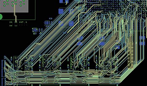
Signal integrity is crucial in LVDS PCB design, as it ensures that the transmitted signals maintain their quality and timing characteristics, minimizing distortion, jitter, and bit errors. Proper PCB layout techniques are essential to achieve optimal signal integrity in LVDS designs.
Key Considerations for LVDS PCB Layout
Differential Pair Routing
One of the most important aspects of LVDS PCB layout is the proper routing of differential pairs. Follow these guidelines for optimal differential pair routing:
-
Route differential pairs together: Always route the two traces of a differential pair closely together, maintaining a constant spacing between them. This helps to maintain the differential signal’s balance and minimizes crosstalk.
-
Maintain controlled impedance: Ensure that the differential pair’s impedance matches the required characteristic impedance (usually 100Ω for LVDS). This can be achieved by adjusting the trace width, spacing, and the distance to the reference plane.
-
Avoid sharp bends: Use smooth, gradual bends when routing differential pairs to minimize reflections and maintain signal integrity. The bend radius should be at least 3 times the trace width.
-
Minimize skew: Keep the length of the two traces in a differential pair equal to minimize skew. Skew can cause timing issues and degrade signal quality.
Termination and Impedance Matching
Proper termination and impedance matching are critical for maintaining signal integrity in LVDS designs. Consider the following:
-
Use parallel termination: Place a 100Ω resistor across the differential pair at the receiver end to match the characteristic impedance and minimize reflections.
-
Avoid stubs: Minimize the use of stubs in the LVDS signal path, as they can cause impedance mismatches and reflections. If stubs are unavoidable, keep them as short as possible (less than 1/10th of the signal wavelength).
-
Maintain consistent impedance: Ensure that the impedance remains consistent throughout the signal path, including connectors, vias, and transitions between layers.
Crosstalk and EMI Reduction
To minimize crosstalk and EMI in LVDS designs, follow these guidelines:
-
Provide adequate spacing: Maintain sufficient spacing between LVDS differential pairs and other signals, especially high-speed digital or switching signals. A minimum spacing of 3 times the trace width is recommended.
-
Use ground shielding: Place ground traces or planes adjacent to LVDS differential pairs to provide shielding and reduce crosstalk from nearby signals.
-
Minimize loop area: Keep the loop area formed by the differential pair and its return path as small as possible to reduce EMI. This can be achieved by placing the differential traces close together and using a continuous ground plane underneath.
Power Supply Decoupling and Filtering
A clean and stable power supply is essential for maintaining LVDS signal integrity. Consider the following:
-
Use decoupling capacitors: Place decoupling capacitors close to the LVDS transmitter and receiver ICs to provide a low-impedance path for high-frequency noise. Use a combination of bulk capacitors (1-10µF) for low-frequency decoupling and ceramic capacitors (0.01-0.1µF) for high-frequency decoupling.
-
Implement power supply filtering: Use ferrite beads or low-pass filters to suppress high-frequency noise on the power supply lines feeding the LVDS ICs.
-
Separate power planes: Use separate power planes for analog and digital circuitry to minimize noise coupling. Ensure that the LVDS ICs have a clean and stable power supply.
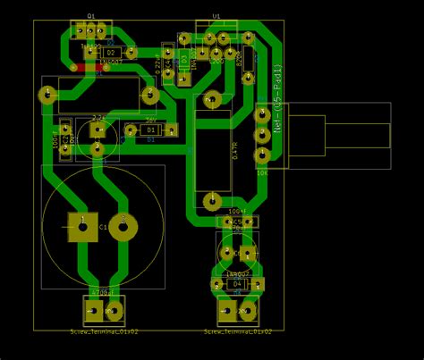
Layer Stack-up and Reference Planes
A well-designed layer stack-up is crucial for maintaining signal integrity in LVDS designs. Consider the following:
-
Use a multi-layer board: A minimum of 4 layers is recommended for LVDS designs, with dedicated signal, ground, and power planes.
-
Provide continuous reference planes: Use continuous ground and power planes to provide a low-impedance return path for the LVDS signals. This helps to minimize EMI and maintain signal integrity.
-
Minimize layer transitions: Avoid unnecessary layer transitions for LVDS signals, as they can cause impedance discontinuities and reflections. If layer transitions are necessary, use vias with appropriate size and placement to minimize their impact.
Length Matching and Skew Control
To ensure proper timing and minimize skew in LVDS designs, follow these guidelines:
-
Match trace lengths: Keep the length of the traces in a differential pair equal to minimize skew. If length matching is not possible, ensure that the skew is within the acceptable limits specified by the LVDS standard (usually less than 50ps).
-
Consider serpentine routing: If necessary, use serpentine routing to match the lengths of the traces in a differential pair. However, be cautious when using serpentines, as they can introduce impedance discontinuities and reflections if not designed properly.
-
Minimize propagation delay differences: Ensure that the propagation delay differences between LVDS pairs are within the acceptable limits. This is particularly important for applications that require synchronization between multiple LVDS channels.
LVDS PCB Layout Techniques
Differential Pair Routing Techniques
| Technique | Description | Advantages | Disadvantages |
|---|---|---|---|
| Edge-coupled | Traces routed side-by-side | Easy to route, good coupling | Requires more space |
| Broadside-coupled | Traces routed on adjacent layers | Saves space, excellent coupling | Requires tight control of layer spacing |
| Coplanar waveguide | Traces routed with ground traces on either side | Good shielding, controlled impedance | Requires more space, complex to route |
Via Placement and Optimization
- Place vias close to the LVDS ICs to minimize stub lengths
- Use via-in-pad or microvias for high-density designs
- Optimize via size and anti-pad diameter for impedance matching
- Avoid unnecessary layer transitions and keep via count low
Connector and Cable Considerations
- Choose connectors and cables rated for LVDS signaling
- Ensure proper impedance matching between the PCB and the connector/cable
- Minimize cable length to reduce signal degradation and EMI
- Use shielded cables for improved noise immunity

LVDS PCB Layout Simulation and Verification
To ensure the integrity of LVDS signals in your PCB design, it is essential to perform simulations and verifications. Some common simulation and verification techniques include:
-
Signal integrity simulations: Use specialized software to simulate the behavior of LVDS signals in your PCB layout. This can help identify potential issues like reflections, crosstalk, and skew.
-
Impedance calculations: Calculate the impedance of your differential pairs to ensure they match the required characteristic impedance. Many PCB design tools have built-in calculators for this purpose.
-
Design rule checks (DRC): Run DRC on your PCB layout to check for violations of the LVDS layout guidelines, such as minimum spacing, trace width, and via size.
-
Time-domain reflectometry (TDR): Use TDR measurements to verify the impedance profile of your LVDS signal paths and identify any discontinuities or mismatches.
-
Eye diagram analysis: Perform eye diagram measurements on your LVDS signals to assess the signal quality and ensure that the eye opening meets the required specifications.
By incorporating these simulation and verification techniques into your LVDS PCB design process, you can identify and address potential signal integrity issues early, saving time and cost in the long run.
Best Practices for LVDS PCB Layout
To summarize the key points for ensuring signal integrity in LVDS PCB layouts, follow these best practices:
- Route differential pairs closely together with a constant spacing
- Maintain controlled impedance throughout the signal path
- Use smooth, gradual bends and avoid sharp corners
- Minimize skew by keeping trace lengths equal
- Use parallel termination at the receiver end
- Avoid stubs and minimize their length when unavoidable
- Provide adequate spacing between LVDS pairs and other signals
- Use ground shielding to reduce crosstalk and EMI
- Implement proper power supply decoupling and filtering
- Use a multi-layer board with dedicated signal, ground, and power planes
- Minimize layer transitions and optimize via placement
- Perform signal integrity simulations and verifications
By adhering to these guidelines, you can ensure optimal signal integrity in your LVDS PCB designs, resulting in reliable and high-performance systems.
Frequently Asked Questions (FAQ)
- What is the recommended characteristic impedance for LVDS differential pairs?
-
The recommended characteristic impedance for LVDS differential pairs is 100Ω.
-
How closely should I route the traces in an LVDS differential pair?
-
The traces in an LVDS differential pair should be routed as closely together as possible, maintaining a constant spacing between them. The spacing should be determined based on the required characteristic impedance and the PCB stack-up.
-
What is the maximum allowable skew between the traces in an LVDS differential pair?
-
The maximum allowable skew between the traces in an LVDS differential pair is usually less than 50ps, as specified by the LVDS standard. However, it is best to minimize skew as much as possible for optimal signal integrity.
-
What type of termination should I use for LVDS signals?
-
LVDS signals should use parallel termination, with a 100Ω resistor placed across the differential pair at the receiver end. This helps to match the characteristic impedance and minimize reflections.
-
How can I reduce crosstalk and EMI in my LVDS PCB layout?
- To reduce crosstalk and EMI in your LVDS PCB layout, provide adequate spacing between LVDS differential pairs and other signals, use ground shielding, and minimize the loop area formed by the differential pair and its return path. Additionally, ensure proper power supply decoupling and filtering to minimize noise coupling.
Conclusion
Designing a PCB layout for LVDS signals requires careful consideration of various factors to ensure optimal signal integrity. By following the guidelines and best practices outlined in this article, you can create robust and reliable LVDS designs that minimize signal distortion, jitter, and bit errors.
Remember to focus on proper differential pair routing, impedance matching, crosstalk and EMI reduction, power supply decoupling, and layer stack-up design. Additionally, performing signal integrity simulations and verifications can help you identify and address potential issues early in the design process.
By adhering to these LVDS PCB layout guidelines, you can ensure that your high-speed designs perform optimally, leading to successful and efficient implementations in a wide range of applications.
No responses yet