Introduction to Soldermask and CTI
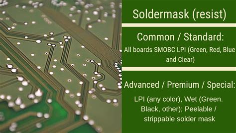
Soldermask, also known as solder resist, is a thin layer of polymer applied to the surface of a printed circuit board (PCB) to protect the copper traces from oxidation and prevent solder bridges during the soldering process. It also provides electrical insulation and helps to prevent short circuits. The soldermask is usually green in color, but other colors like red, blue, black, and white are also available.
Comparative Tracking Index (CTI) is a measure of the electrical breakdown properties of an insulating material. It is used to determine the ability of a material to resist electrical tracking, which can lead to short circuits and other electrical failures. CTI is measured according to the IEC 60112 standard, and materials are classified into one of four categories based on their CTI value:
| CTI Category | CTI Value Range |
|---|---|
| 0 | CTI ≤ 175 |
| 1 | 175 < CTI ≤ 400 |
| 2 | 400 < CTI ≤ 600 |
| 3 | CTI > 600 |
High CTI boards, also known as high-voltage boards, are PCBs that are designed to operate at high voltages (typically above 1000V) and require a soldermask with a high CTI value to ensure reliable operation and prevent electrical failures.
Importance of High CTI Soldermask
High CTI soldermask is essential for high-voltage applications because it provides the necessary electrical insulation and prevents electrical tracking. Some of the key benefits of using high CTI soldermask include:
-
Improved electrical insulation: High CTI soldermask provides better electrical insulation than standard soldermask, which helps to prevent short circuits and other electrical failures.
-
Increased reliability: By preventing electrical tracking and other failures, high CTI soldermask helps to increase the reliability of High-Voltage PCBs.
-
Enhanced safety: High CTI soldermask helps to ensure the safety of operators and equipment by preventing electrical shocks and other hazards.
-
Compliance with industry standards: Many industries, such as automotive, aerospace, and medical, have strict requirements for the CTI value of soldermask used in high-voltage applications. Using high CTI soldermask ensures compliance with these standards.
Factors Affecting Soldermask CTI
Several factors can affect the CTI value of soldermask, including:
Material Composition
The chemical composition of the soldermask material is one of the primary factors that determine its CTI value. Soldermask materials with higher levels of inorganic fillers, such as silica or alumina, tend to have higher CTI values than those with lower levels of fillers.
Thickness
The thickness of the soldermask layer can also affect its CTI value. Thicker soldermask layers generally have higher CTI values than thinner layers, as they provide better electrical insulation and are more resistant to electrical tracking.
Surface Roughness
The surface roughness of the soldermask can also impact its CTI value. Smoother surfaces tend to have higher CTI values than rougher surfaces, as they are less prone to electrical tracking and other failures.
Environmental Factors
Environmental factors, such as temperature, humidity, and contaminants, can also affect the CTI value of soldermask. High temperatures and humidity can degrade the electrical insulation properties of soldermask, while contaminants like dust and oils can create a conductive path that leads to electrical tracking.

Soldermask Selection for High CTI Boards
When selecting a soldermask for high CTI boards, several factors should be considered, including:
CTI Value
The most important factor to consider when selecting a soldermask for high CTI boards is the CTI value. The soldermask should have a CTI value that meets or exceeds the requirements for the specific application. For example, the automotive industry typically requires a minimum CTI value of 600 for high-voltage applications.
Compatibility with PCB Materials
The soldermask must be compatible with the PCB materials used, including the substrate, copper traces, and any other components or coatings. Incompatible materials can lead to adhesion problems, delamination, or other failures.
Processing Requirements
The soldermask must be able to withstand the processing requirements of the PCB manufacturing process, including exposure to high temperatures during soldering and any cleaning or post-processing steps.
Cost and Availability
The cost and availability of the soldermask should also be considered, as high CTI soldermasks may be more expensive or have longer lead times than standard soldermasks.
Application Methods for High CTI Soldermask
There are several methods for applying high CTI soldermask to PCBs, including:
Screen Printing
Screen printing is the most common method for applying soldermask to PCBs. It involves using a stencil to apply the soldermask material to the PCB surface, followed by curing with UV light or heat. Screen printing is suitable for most PCB Designs and can achieve a consistent soldermask thickness.
Liquid Photoimageable (LPI)
LPI soldermask is applied as a liquid and then exposed to UV light through a photomask to selectively cure the soldermask in the desired areas. LPI soldermask provides high resolution and can accommodate fine pitch components and traces.
Dry Film Photoimageable
Dry film photoimageable soldermask is applied as a solid film and then exposed to UV light through a photomask, similar to LPI soldermask. Dry film soldermask is suitable for high-volume production and can provide a consistent soldermask thickness.
Testing and Qualification of High CTI Soldermask
To ensure that the high CTI soldermask meets the required performance and reliability standards, several tests and qualifications are typically performed, including:
CTI Testing
CTI testing is performed according to the IEC 60112 standard to determine the CTI value of the soldermask. The test involves applying a voltage across a specified gap on the soldermask surface and gradually increasing the voltage until electrical tracking occurs.
Adhesion Testing
Adhesion testing is performed to ensure that the soldermask adheres properly to the PCB surface and does not delaminate during processing or use. Adhesion testing typically involves performing a cross-hatch test or a tape test.
Environmental Testing
Environmental testing is performed to ensure that the soldermask can withstand the expected environmental conditions, such as temperature, humidity, and chemical exposure. Common environmental tests include thermal cycling, damp heat, and salt spray testing.
Electrical Testing
Electrical testing is performed to ensure that the soldermask provides adequate electrical insulation and does not break down under high voltage stress. Common electrical tests include dielectric withstanding voltage (DWV) testing and insulation resistance testing.
FAQs
-
What is the difference between standard soldermask and high CTI soldermask?
Standard soldermask is designed for general-purpose applications and typically has a lower CTI value than high CTI soldermask. High CTI soldermask is specifically designed for high-voltage applications and has a higher CTI value, providing better electrical insulation and resistance to electrical tracking. -
What is the minimum CTI value required for high-voltage applications?
The minimum CTI value required for high-voltage applications varies depending on the specific industry and application. For example, the automotive industry typically requires a minimum CTI value of 600 for high-voltage applications, while other industries may have different requirements. -
Can high CTI soldermask be applied using the same methods as standard soldermask?
Yes, high CTI soldermask can be applied using the same methods as standard soldermask, including screen printing, liquid photoimageable (LPI), and dry film photoimageable. However, the specific processing parameters, such as curing time and temperature, may need to be adjusted to ensure proper curing and adhesion of the high CTI soldermask. -
How does the thickness of the soldermask affect its CTI value?
Thicker soldermask layers generally have higher CTI values than thinner layers, as they provide better electrical insulation and are more resistant to electrical tracking. However, increasing the soldermask thickness may also increase the cost and processing time of the PCB. -
What environmental factors can affect the CTI value of soldermask?
Environmental factors that can affect the CTI value of soldermask include temperature, humidity, and contaminants. High temperatures and humidity can degrade the electrical insulation properties of soldermask, while contaminants like dust and oils can create a conductive path that leads to electrical tracking. To ensure reliable performance, high CTI boards should be designed and tested to withstand the expected environmental conditions.
Conclusion
High CTI soldermask is essential for ensuring the reliability and safety of high-voltage PCBs. When selecting a soldermask for high CTI boards, it is important to consider factors such as the CTI value, compatibility with PCB materials, processing requirements, and cost and availability. Proper application and testing of the soldermask are also critical to ensure that it meets the required performance and reliability standards.
By understanding the requirements and best practices for high CTI soldermask, PCB Designers and manufacturers can ensure that their high-voltage boards are reliable, safe, and compliant with industry standards.
No responses yet