Introduction to SMT Stencils
Surface Mount Technology (SMT) has revolutionized the electronics manufacturing industry by enabling the production of smaller, faster, and more efficient electronic devices. One of the key components in the SMT process is the Solder paste stencil, also known as the SMT stencil. This article will provide an in-depth look at SMT stencils, their importance, types, materials, design considerations, and best practices for optimal results.
What is an SMT Stencil?
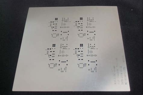
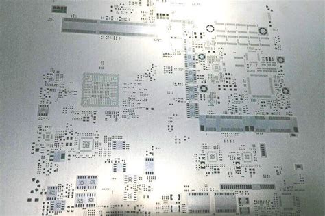
An SMT stencil is a thin, flat sheet of material with precisely cut apertures that correspond to the pads on a printed circuit board (PCB). The stencil is used to apply solder paste onto the PCB pads before placing the surface mount components. The solder paste deposited through the stencil apertures ensures a precise and consistent amount of solder is applied to each pad, resulting in reliable solder joints after the reflow process.
Importance of SMT Stencils in Electronics Manufacturing
SMT stencils play a crucial role in the electronics manufacturing process by:
- Ensuring precise solder paste deposition
- Maintaining consistent solder joint quality
- Enabling high-volume production
- Reducing assembly errors and defects
- Facilitating the use of smaller components and fine-pitch devices
Types of SMT Stencils
There are several types of SMT stencils available, each with its own advantages and applications.
Laser-Cut Stencils
Laser-cut stencils are created using a high-precision laser to cut apertures into a thin sheet of stainless steel. This process allows for highly accurate and complex aperture designs, making laser-cut stencils suitable for fine-pitch and high-density PCB assemblies. Laser-cut stencils are durable and can be used for multiple print cycles, making them a cost-effective option for high-volume production.
Electroformed Stencils
Electroformed stencils, also known as E-FAB stencils, are created using an electrochemical process that deposits nickel onto a photoresist-patterned substrate. This process results in a stencil with smooth, tapered aperture walls, which promotes better paste release and reduces the risk of bridging. Electroformed stencils are ideal for ultra-fine pitch applications and can achieve aperture sizes as small as 0.05mm.
Nano-Coated Stencils
Nano-coated stencils feature a thin, hydrophobic coating applied to the surface of the stencil. This coating prevents solder paste from sticking to the stencil, improving paste release and reducing the need for frequent cleaning. Nano-coated stencils are particularly useful for high-volume production runs and can help maintain consistent print quality over extended periods.
SMT Stencil Materials
SMT stencils are typically made from one of two materials: stainless steel or nickel.
Stainless Steel Stencils
Stainless steel is the most common material used for SMT stencils due to its durability, stability, and cost-effectiveness. Stainless steel stencils are available in various thicknesses, ranging from 0.076mm to 0.2mm (3-8 mils), to accommodate different solder paste deposition requirements. These stencils are compatible with both laser cutting and chemical etching processes.
Nickel Stencils
Nickel stencils, primarily used in electroformed stencils, offer several advantages over stainless steel. Nickel has a lower surface energy than stainless steel, which promotes better solder paste release and reduces the risk of clogging. Additionally, nickel stencils can achieve finer aperture sizes and more intricate designs due to the electroforming process. However, nickel stencils are generally more expensive than stainless steel stencils.

SMT Stencil Design Considerations
Designing an effective SMT stencil requires careful consideration of several factors to ensure optimal solder paste deposition and assembly quality.
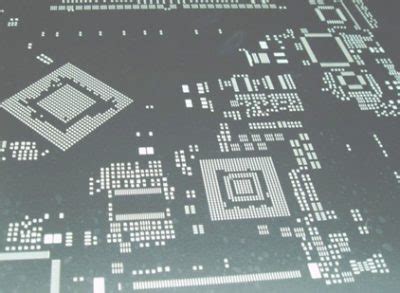
Aperture Size and Shape
Aperture size and shape are critical aspects of SMT stencil design. The aperture size should be slightly larger than the PCB pad to allow for proper solder paste coverage. However, oversized apertures can lead to excessive solder paste deposition, resulting in bridging and other defects. Aperture shape also plays a role in solder paste release, with rounded corners and tapered walls promoting better release than sharp corners and straight walls.
Stencil Thickness
Stencil thickness determines the volume of solder paste deposited onto the PCB pads. Thicker stencils deposit more solder paste, which is suitable for larger components and pads. Thinner stencils are used for smaller components and fine-pitch applications to prevent bridging and other defects. The following table provides general guidelines for selecting stencil thickness based on component pitch:
| Component Pitch | Recommended Stencil Thickness |
|---|---|
| > 0.65mm | 0.15mm – 0.2mm (6-8 mils) |
| 0.5mm – 0.65mm | 0.127mm – 0.15mm (5-6 mils) |
| 0.4mm – 0.5mm | 0.1mm – 0.127mm (4-5 mils) |
| < 0.4mm | 0.076mm – 0.1mm (3-4 mils) |
Aperture Aspect Ratio
The aperture aspect ratio is the relationship between the aperture width and the stencil thickness. A higher aspect ratio (larger aperture width relative to stencil thickness) promotes better solder paste release, while a lower aspect ratio can lead to clogging and inconsistent deposition. As a general rule, the aspect ratio should be between 1.5 and 2.0 for optimal results.
Stencil Fabrication and Tolerances
SMT stencil Fabrication tolerances are essential for ensuring accurate and consistent solder paste deposition. The following table outlines typical fabrication tolerances for laser-cut and electroformed stencils:
| Stencil Type | Aperture Size Tolerance | Aperture Position Tolerance |
|---|---|---|
| Laser-cut | ±0.025mm | ±0.05mm |
| Electroformed | ±0.01mm | ±0.025mm |
It is crucial to work closely with your stencil manufacturer to ensure that the fabrication process meets your specific requirements and tolerances.
Best Practices for SMT Stencil Usage
To achieve the best results with SMT stencils, consider the following best practices:
-
Stencil Cleaning: Regularly clean your stencil to remove excess solder paste and prevent clogging. Use a compatible cleaning solution and follow the manufacturer’s recommendations for cleaning frequency and method.
-
Stencil Storage: Store your stencils in a clean, dry environment to prevent damage and contamination. Use a stencil storage rack or container to keep the stencils organized and protected.
-
Print Parameters: Optimize your print parameters, such as print speed, pressure, and separation speed, to ensure consistent solder paste deposition. Conduct regular print tests and adjust parameters as needed.
-
Stencil Inspection: Periodically inspect your stencils for signs of wear, damage, or clogging. Replace stencils as necessary to maintain print quality and prevent defects.
-
Solder Paste Selection: Choose a solder paste that is compatible with your stencil and PCB Design. Consider factors such as particle size, viscosity, and flux chemistry to ensure optimal performance.
Frequently Asked Questions (FAQ)
1. How often should I clean my SMT stencil?
The frequency of stencil cleaning depends on factors such as the solder paste type, print volume, and environmental conditions. As a general guideline, clean your stencil every 4-8 hours of continuous printing or whenever print quality begins to deteriorate.
2. Can I reuse a damaged or worn SMT stencil?
It is not recommended to reuse a damaged or worn SMT stencil, as this can lead to inconsistent solder paste deposition and assembly defects. Replace the stencil as soon as signs of damage or excessive wear are observed.
3. How do I store my SMT stencils when not in use?
Store your SMT stencils in a clean, dry environment, away from direct sunlight and extreme temperatures. Use a stencil storage rack or container to keep the stencils organized and protected from damage.
4. What is the typical lifespan of an SMT stencil?
The lifespan of an SMT stencil depends on factors such as the stencil material, usage frequency, and maintenance practices. A well-maintained stainless steel stencil can last for 20,000-50,000 print cycles, while an electroformed nickel stencil may last up to 100,000 print cycles.
5. Can I use the same SMT stencil for different PCB designs?
Using the same SMT stencil for different PCB designs is not recommended, as each design has unique pad sizes, shapes, and layouts. Using a stencil designed for a specific PCB ensures optimal solder paste deposition and assembly quality.
Conclusion
SMT stencils are a critical component in the electronics manufacturing process, ensuring precise and consistent solder paste deposition for reliable solder joints. Understanding the types of stencils, materials, design considerations, and best practices is essential for achieving optimal results and minimizing assembly defects.
By selecting the appropriate stencil type, material, and thickness for your specific application, and following best practices for stencil usage and maintenance, you can maximize the efficiency and quality of your SMT assembly process. Regularly review your stencil design and performance, and work closely with your stencil manufacturer to ensure that your stencils meet your evolving production requirements.
No responses yet