Introduction to Solder Bridge Jumpers
Solder bridge jumpers are an essential component in printed circuit board (PCB) design. They provide a convenient and reversible way to connect or disconnect specific circuits on a PCB, allowing for customization, testing, and debugging. In this comprehensive article, we will explore the best practices for incorporating solder bridge jumpers in your PCB design to ensure optimal functionality, reliability, and ease of use.
What is a Solder Bridge Jumper?
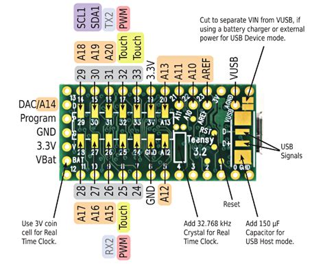
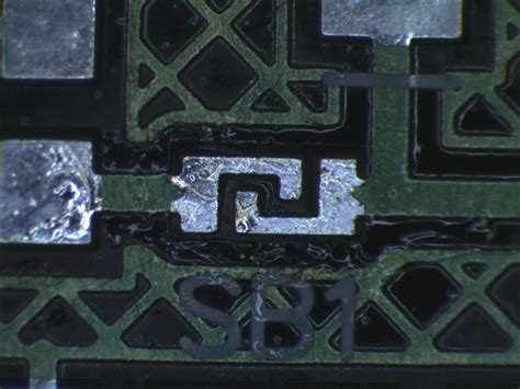
A solder bridge jumper, also known as a solder jumper or zero ohm resistor, is a small component that acts as a switch on a PCB. It consists of two pads connected by a thin trace of conductive material, typically copper. When the jumper is “closed” or “shorted,” it allows electrical current to flow between the two pads, effectively connecting the circuits. Conversely, when the jumper is “open,” it breaks the connection, isolating the circuits from each other.
Solder bridge jumpers offer several advantages over other types of switches:
- Low cost and simplicity: Solder jumpers are inexpensive and easy to incorporate into PCB designs.
- Compact size: They take up minimal space on the board, making them ideal for dense designs.
- Reversibility: Jumpers can be easily opened or closed by adding or removing solder, allowing for modifications and troubleshooting.
When to Use Solder Bridge Jumpers
Solder bridge jumpers find applications in various scenarios:
-
Configuration settings: Jumpers can be used to select different operating modes, such as voltage levels, communication protocols, or device addresses.
-
Feature selection: They can enable or disable specific features of a device, such as pull-up resistors, termination resistors, or bypass capacitors.
-
Debugging and testing: Jumpers facilitate access to test points or allow isolation of specific sections of the circuit for troubleshooting purposes.
-
Manufacturing options: They can be used to create different product variants from a single PCB design by selectively populating or depopulating jumpers.

Best Practices for Solder Bridge Jumper Design
To ensure optimal performance and usability of solder bridge jumpers in your PCB design, consider the following best practices:
Pad Size and Spacing
The pad size and spacing of solder jumpers should be carefully chosen to ensure ease of soldering and prevent accidental bridging. Typical pad sizes range from 0.5mm to 1.5mm in diameter, with a spacing of 0.2mm to 0.5mm between pads. Larger pads and wider spacing make manual soldering easier, while smaller pads allow for denser designs.
| Pad Size (mm) | Spacing (mm) | Soldering Difficulty | Density |
|---|---|---|---|
| 0.5 – 0.8 | 0.2 – 0.3 | High | High |
| 0.8 – 1.2 | 0.3 – 0.4 | Medium | Medium |
| 1.2 – 1.5 | 0.4 – 0.5 | Low | Low |
Trace Width and Length
The trace connecting the pads should be wide enough to handle the expected current flow without excessive heating. A typical trace width of 0.2mm to 0.5mm is sufficient for most applications. The trace length should be kept as short as possible to minimize resistance and inductance.
Solder Mask Opening
A solder mask opening should be provided around the jumper pads to prevent solder bridging to adjacent components or traces. The opening should be slightly larger than the pad size, typically by 0.1mm to 0.2mm on all sides.
Silkscreen Labeling
Clear and concise labeling of solder jumpers on the silkscreen layer is crucial for easy identification and configuration. Use descriptive text or symbols to indicate the function of each jumper, such as “VCC_SEL” or “I2C_ADDR.” Include a label for the open and closed positions, such as “O” and “C,” or “1” and “2.”
Placement and Orientation
Solder jumpers should be placed in easily accessible locations on the PCB, preferably near the edge of the board or in dedicated configuration areas. Orient the jumpers consistently, either horizontally or vertically, to avoid confusion. Consider the placement of other components and connectors to ensure sufficient clearance for soldering and manipulation.
Jumper Variants
In some cases, it may be beneficial to use specialized jumper variants:
-
Three-pad jumpers: These jumpers have an additional pad in the middle, allowing for three different configuration options.
-
Castellated jumpers: These jumpers have castellated holes instead of pads, making them compatible with pin headers for improved mechanical stability.
-
Surface-mount jumpers: These jumpers are designed for automated assembly and have a low profile, making them suitable for space-constrained designs.
Solder Bridge Jumper Assembly and Modification
Manual Soldering
To close a solder jumper manually, apply a small amount of solder across the pads using a fine-tipped soldering iron. Use a solder wire with a diameter of 0.5mm to 0.8mm and a low-temperature solder alloy, such as Sn63Pb37 or Sn96.5Ag3.0Cu0.5. To open a jumper, carefully remove the solder bridge using solder wick or a solder sucker.
Automated Assembly
For automated assembly, solder paste can be applied to the jumper pads using stencil printing or dispensing. The jumpers can then be placed and reflowed along with other surface-mount components. To leave a jumper open, simply omit the solder paste on its pads.
Jumper Modification
If a jumper needs to be modified after assembly, follow these steps:
- Heat the solder bridge with a soldering iron until it melts.
- Use solder wick or a solder sucker to remove the molten solder.
- Clean the pads with isopropyl alcohol to remove any residue.
- To close the jumper again, apply fresh solder as described in the manual soldering section.
PCB Layout Considerations
When incorporating solder bridge jumpers into your PCB layout, keep the following considerations in mind:
-
Avoid placing jumpers under other components or in areas that are difficult to access with a soldering iron.
-
Provide sufficient clearance around jumpers for soldering and inspection.
-
Keep jumpers away from high-frequency or sensitive analog circuits to prevent interference.
-
Consider the potential impact of jumper modifications on signal integrity and impedance matching.
-
Include jumper configuration information in the assembly drawing and bill of materials (BOM) to ensure correct assembly.
Frequently Asked Questions (FAQ)
1. What is the difference between a solder bridge jumper and a zero ohm resistor?
A solder bridge jumper and a zero ohm resistor serve the same purpose of connecting two points on a PCB. However, a zero ohm resistor is a discrete component that is placed on the board during assembly, while a solder bridge jumper is a pad and trace feature that is part of the PCB design itself. Zero ohm resistors are more suitable for automated assembly, while solder bridge jumpers offer more flexibility for manual modifications.
2. Can solder bridge jumpers handle high currents?
The current-carrying capacity of a solder bridge jumper depends on the trace width and the solder alloy used. For high-current applications, use wider traces and high-temperature solder alloys. Consult the trace width calculators and solder specifications to determine the suitable dimensions and materials for your specific requirements.
3. How do I ensure reliable solder bridge jumper connections?
To ensure reliable jumper connections, use clean and properly sized soldering tools, apply the right amount of solder, and follow good soldering techniques. Inspect the jumper connections visually and with a multimeter to verify continuity and the absence of shorts. If needed, clean the jumper pads and reflow the solder to improve the connection quality.
4. Can solder bridge jumpers be used in high-frequency circuits?
Solder bridge jumpers can be used in high-frequency circuits, but their placement and design should be carefully considered. Keep the jumper traces as short as possible to minimize inductance and avoid placing them near sensitive signal paths. In some cases, it may be better to use a dedicated high-frequency switch or a zero ohm resistor with controlled impedance.
5. Are there any automated methods for modifying solder bridge jumpers?
Yes, automated methods for modifying solder bridge jumpers exist, such as robotic soldering systems or laser cutters. These methods are typically used in high-volume production or for jumpers that are difficult to access manually. However, they require specialized equipment and programming, making them less suitable for small-scale or prototype projects.
Conclusion
Solder bridge jumpers are a versatile and cost-effective solution for configuring, testing, and debugging PCBs. By following the best practices outlined in this article, you can incorporate solder jumpers into your PCB design with confidence, ensuring optimal performance and ease of use. Remember to consider pad size and spacing, trace dimensions, solder mask openings, silkscreen labeling, and placement when designing your jumpers. During assembly and modification, use the appropriate tools and techniques to achieve reliable and robust connections.
As with any PCB design element, solder bridge jumpers should be used judiciously and in accordance with the specific requirements of your project. By understanding their strengths and limitations, you can leverage solder jumpers effectively to create flexible, adaptable, and maintainable electronic devices.
No responses yet