Introduction to Solder Bridges
Soldering is a crucial process in the assembly and manufacturing of electronic devices, where components are connected to a printed circuit board (PCB) using molten metal alloy, typically a tin-lead mixture. While soldering is essential for creating reliable electrical connections, it can also lead to unintended issues, such as solder bridges.
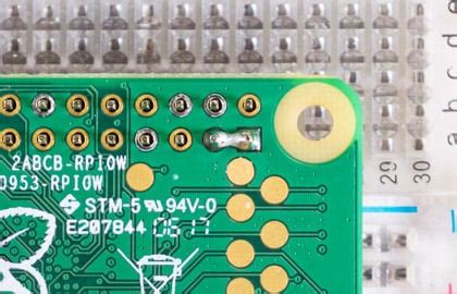
A solder bridge is an unwanted connection formed between two adjacent pads or traces on a PCB due to excess solder. This unintentional connection can cause short circuits, leading to malfunctions or even permanent damage to the electronic device.
Understanding the Causes of Solder Bridges
Several factors can contribute to the formation of solder bridges during the soldering process:
- Excessive solder: Applying too much solder can cause it to overflow and create a connection between adjacent pads.
- Improper soldering technique: Poor soldering skills, such as holding the soldering iron at the wrong angle or for too long, can result in solder bridges.
- Inadequate PCB design: If the pads or traces on a PCB are too close together, it increases the likelihood of solder bridges forming.
- Contamination: Dirt, dust, or other contaminants on the PCB surface can interfere with the soldering process and lead to bridges.
Identifying Solder Bridges
Detecting solder bridges is crucial for ensuring the proper functioning of electronic devices. There are several methods to identify the presence of solder bridges:
Visual Inspection
The most straightforward method to identify solder bridges is through visual inspection. By carefully examining the soldered components and pads using a magnifying glass or microscope, you can spot any unwanted connections between adjacent pads.
Look for the following signs of solder bridges during visual inspection:
- Excess solder forming a connection between two pads
- Solder splatter or droplets on the PCB surface
- Uneven or bulging solder joints
Continuity Testing
Continuity testing is an effective way to detect solder bridges that may not be visible to the naked eye. This method involves using a multimeter to check for electrical continuity between two points on the PCB that should not be connected.
To perform continuity testing:
- Set the multimeter to the continuity or resistance mode.
- Place one probe on a pad or trace and the other probe on an adjacent pad or trace.
- If the multimeter beeps or indicates a low resistance, it suggests the presence of a solder bridge.
Functional Testing
Functional testing involves powering up the electronic device and checking for any abnormal behavior or malfunctions. Solder bridges can cause short circuits, leading to issues such as:
- The device not turning on
- Erratic or unexpected behavior
- Overheating of components
- Burning smell or visible smoke
If any of these symptoms are observed during functional testing, it may indicate the presence of a solder bridge.

Preventing Solder Bridges
Preventing solder bridges is essential for ensuring the reliability and longevity of electronic devices. Here are some best practices to minimize the occurrence of solder bridges:
Proper Soldering Technique
Using the correct soldering technique is crucial for preventing solder bridges. Follow these guidelines:
- Use an appropriately sized soldering iron tip for the job
- Apply the right amount of solder, avoiding excess
- Keep the soldering iron at the correct angle and distance from the joint
- Maintain a steady hand and avoid sudden movements
PCB Design Considerations
Proper PCB design can help reduce the likelihood of solder bridges forming. Consider the following:
- Ensure adequate spacing between pads and traces
- Use solder mask to cover areas where solder is not intended to flow
- Implement design for manufacturability (DFM) principles to optimize the PCB layout
Cleaning and Maintenance
Regularly cleaning and maintaining the soldering equipment and workspace can help prevent contamination that may lead to solder bridges. Follow these practices:
- Keep the soldering iron tip clean and tinned
- Use a clean, static-free work surface
- Remove any flux residue or debris from the PCB after soldering
- Store components and PCBs in a clean, dry environment

Repairing Solder Bridges
If a solder bridge is detected, it is essential to repair it promptly to avoid potential damage to the electronic device. The following methods can be used to remove solder bridges:
Solder Wick
Solder wick, also known as desoldering braid, is a copper braid coated with flux that is used to absorb excess solder. To remove a solder bridge using solder wick:
- Place the solder wick on the solder bridge.
- Apply the soldering iron to the wick, allowing it to heat up and absorb the excess solder.
- Lift the soldering iron and wick away from the PCB once the solder bridge is removed.
Desoldering Pump
A desoldering pump, or solder sucker, is a spring-loaded tool that uses suction to remove molten solder. To use a desoldering pump:
- Heat the solder bridge with the soldering iron.
- Place the desoldering pump nozzle near the molten solder.
- Activate the pump to suck up the excess solder.
Soldering Iron
In some cases, a solder bridge can be removed using just a soldering iron. To do this:
- Heat the solder bridge with the soldering iron tip.
- Gently drag the tip between the two pads to separate the solder bridge.
- Remove any remaining excess solder using solder wick or a desoldering pump.

Conclusion
Solder bridges are a common issue in electronic assembly that can lead to malfunctions and damage to devices. Understanding the causes, identification methods, prevention techniques, and repair processes is crucial for ensuring the reliability and longevity of electronic products.
By implementing best practices in soldering techniques, PCB design, and maintenance, the occurrence of solder bridges can be minimized. When solder bridges are detected, prompt repair using methods such as solder wick, desoldering pumps, or soldering irons can prevent further damage and ensure the proper functioning of the electronic device.
Frequently Asked Questions (FAQ)
-
What is a solder bridge?
A solder bridge is an unintended connection formed between two adjacent pads or traces on a PCB due to excess solder. -
What causes solder bridges?
Solder bridges can be caused by excessive solder application, improper soldering technique, inadequate PCB design, or contamination on the PCB surface. -
How can I identify solder bridges?
Solder bridges can be identified through visual inspection, continuity testing using a multimeter, or functional testing of the electronic device. -
How can I prevent solder bridges from occurring?
To prevent solder bridges, use proper soldering techniques, ensure adequate spacing between pads and traces in PCB design, and maintain a clean soldering environment. -
What methods can be used to repair solder bridges?
Solder bridges can be repaired using solder wick, desoldering pumps, or soldering irons to remove the excess solder connecting the adjacent pads or traces.
| Method | Advantages | Disadvantages |
|---|---|---|
| Visual Inspection | – Quick and simple – No additional tools required |
– May miss small or hidden solder bridges |
| Continuity Testing | – Detects bridges not visible to the naked eye | – Requires a multimeter – May be time-consuming |
| Functional Testing | – Identifies issues caused by solder bridges | – Potential risk of damage to the device |
Table 1: Comparison of solder bridge identification methods
| Method | Procedure |
|---|---|
| Solder Wick | 1. Place wick on bridge 2. Heat with soldering iron 3. Lift wick to remove solder |
| Desoldering Pump | 1. Heat solder bridge 2. Place pump nozzle near molten solder 3. Activate pump to remove solder |
| Soldering Iron | 1. Heat solder bridge 2. Drag iron tip to separate bridge 3. Remove excess solder |
Table 2: Solder bridge repair methods
By understanding the causes, identification methods, prevention techniques, and repair processes for solder bridges, electronic manufacturers and hobbyists can ensure the reliability and proper functioning of their devices. Implementing best practices in soldering and PCB design, along with regular inspection and maintenance, can significantly reduce the occurrence of solder bridges and improve the overall quality of electronic products.
No responses yet