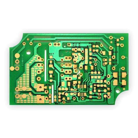
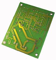
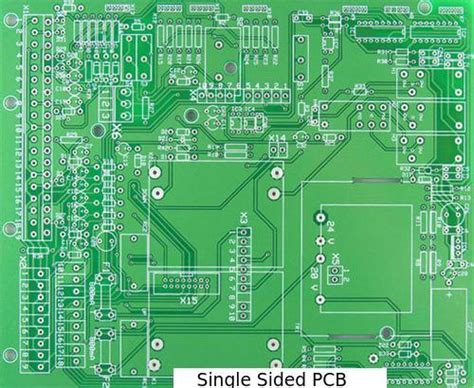
What is a Single-sided PCB?
A single-sided PCB, also known as a single-layer PCB, is a printed circuit board that has conductive copper traces on only one side of the board. The other side of the board is typically left bare or covered with a solder mask to protect against short circuits. Single-sided PCBs are the simplest and most cost-effective type of PCB, making them a popular choice for simple electronic projects and low-cost consumer devices.
Advantages of Single-sided PCBs
- Low cost: Single-sided PCBs are the most affordable type of PCB due to their simple design and manufacturing process.
- Easy to design: With only one layer of copper traces, single-sided PCBs are easier to design compared to multi-layer PCBs.
- Quick turnaround: Single-sided PCBs can be manufactured quickly, making them ideal for rapid prototyping and small production runs.
- Suitable for simple circuits: Single-sided PCBs are perfect for simple electronic projects that do not require complex routing or high component density.
Disadvantages of Single-sided PCBs
- Limited routing options: With only one layer of copper traces, single-sided PCBs have limited routing options, which can make it challenging to route complex circuits.
- Lower component density: Single-sided PCBs cannot accommodate as many components as multi-layer PCBs due to the limited space on one side of the board.
- Reduced electrical performance: Single-sided PCBs may have reduced electrical performance compared to multi-layer PCBs, especially at high frequencies.
- Not suitable for high-power applications: Single-sided PCBs are not recommended for high-power applications due to their limited current carrying capacity and potential for thermal issues.
Single-sided PCB Manufacturing Process
The manufacturing process for single-sided PCBs involves several steps, including:
-
PCB Design: The first step in manufacturing a single-sided PCB is to create a PCB design using CAD software. The design includes the placement of components, routing of copper traces, and the creation of solder pads and vias.
-
Film Generation: Once the PCB design is complete, a photographic film or photomask is created from the design files. This film is used to transfer the PCB design onto the copper-clad board.
-
Copper Etching: The copper-clad board is coated with a light-sensitive resist, and the photomask is placed on top of the board. The board is then exposed to UV light, which hardens the resist where the copper traces will be. The unexposed resist is then removed, leaving behind the copper traces.
-
Solder Mask Application: A solder mask is applied to the board to protect the copper traces from oxidation and to prevent solder bridges during the soldering process. The solder mask is typically green, but other colors are available.
-
Silkscreen Printing: A silkscreen is used to print text, logos, and other markings on the PCB. This helps with component placement and identification during assembly.
-
Surface Finish: A surface finish, such as HASL (Hot Air Solder Leveling) or ENIG (Electroless Nickel Immersion Gold), is applied to the exposed copper pads to prevent oxidation and improve solderability.
-
Drilling: Holes are drilled in the PCB for through-hole components and vias.
-
Electrical Testing: The finished PCB is electrically tested to ensure that all connections are correct and there are no short circuits or open circuits.
Single-sided PCB Design Considerations
When designing a single-sided PCB, there are several key considerations to keep in mind:
Component Placement
Component placement is critical in single-sided PCB design. Components should be placed in a logical order that minimizes the length of copper traces and reduces the number of vias required. It is also important to consider the physical size of the components and ensure that there is adequate spacing between them to prevent short circuits and thermal issues.
Trace Width and Spacing
The width and spacing of copper traces on a single-sided PCB are important factors in determining the current carrying capacity and impedance of the traces. Wider traces can carry more current and have lower impedance, but they also take up more space on the board. Narrower traces have higher impedance and can carry less current, but they allow for denser routing. It is important to carefully consider the trade-offs between trace width and spacing when designing a single-sided PCB.
Vias and Jumpers
Vias and jumpers are used to connect traces on opposite sides of the board in a single-sided PCB design. Vias are small holes drilled through the board that are plated with copper to create an electrical connection between the top and bottom layers. Jumpers are short wires that are soldered between two points on the board to create an electrical connection. While vias and jumpers can be useful for routing complex circuits on a single-sided PCB, they also add cost and complexity to the manufacturing process.
Ground Plane
A ground plane is a large area of copper on the PCB that is connected to the ground potential of the circuit. Ground planes provide a low-impedance return path for current and help to reduce electromagnetic interference (EMI) and improve signal integrity. In a single-sided PCB design, the ground plane is typically placed on the opposite side of the board from the components and traces. It is important to ensure that the ground plane is properly connected to the ground potential of the circuit and that there are adequate vias to connect the ground plane to the components and traces on the top layer.

Single-sided PCB Assembly
Assembling a single-sided PCB is a relatively simple process that can be done by hand or using automated assembly equipment. The basic steps in the assembly process include:
-
Solder Paste Application: Solder paste is applied to the pads on the PCB using a stencil or syringe. The solder paste contains a mixture of tiny solder balls and flux that helps to bond the components to the board.
-
Component Placement: The components are placed on the PCB using tweezers or automated pick-and-place equipment. It is important to ensure that the components are properly aligned with the pads on the board.
-
Reflow Soldering: The PCB is placed in a reflow oven, which heats the board and melts the solder paste. The molten solder flows around the component leads and forms a strong mechanical and electrical bond between the components and the board.
-
Inspection and Testing: After the reflow process is complete, the PCB is inspected visually and electrically to ensure that all components are properly soldered and that there are no defects or short circuits.
Single-sided PCB Applications
Single-sided PCBs are used in a wide range of electronic applications, including:
- Consumer electronics: Single-sided PCBs are commonly used in low-cost consumer electronics, such as toys, remote controls, and simple appliances.
- Prototyping: Single-sided PCBs are often used for prototyping and testing new designs due to their low cost and quick turnaround time.
- Educational projects: Single-sided PCBs are popular in educational settings, such as schools and universities, where students are learning about electronics and PCB design.
- Hobby projects: Many hobbyists and makers use single-sided PCBs for their projects due to their simplicity and low cost.
FAQ
1. What is the difference between a single-sided and double-sided PCB?
A single-sided PCB has conductive copper traces on only one side of the board, while a double-sided PCB has copper traces on both sides of the board. Double-sided PCBs offer more routing options and higher component density compared to single-sided PCBs, but they are also more expensive and complex to manufacture.
2. Can single-sided PCBs be used for high-frequency applications?
Single-sided PCBs are generally not recommended for high-frequency applications due to their limited routing options and potential for signal integrity issues. For high-frequency applications, multi-layer PCBs with controlled impedance and dedicated power and ground planes are typically used.
3. What is the maximum number of components that can be placed on a single-sided PCB?
The maximum number of components that can be placed on a single-sided PCB depends on several factors, including the size of the board, the size of the components, and the complexity of the circuit. In general, single-sided PCBs are limited to a few dozen components, while multi-layer PCBs can accommodate hundreds or even thousands of components.
4. Can single-sided PCBs be manufactured using the same equipment as multi-layer PCBs?
Yes, single-sided PCBs can be manufactured using the same equipment as multi-layer PCBs, including etching machines, drilling machines, and solder mask application equipment. However, the manufacturing process for single-sided PCBs is generally simpler and faster compared to multi-layer PCBs.
5. What are some common design mistakes to avoid when creating a single-sided PCB?
Some common design mistakes to avoid when creating a single-sided PCB include:
- Placing components too close together, which can lead to short circuits and thermal issues.
- Using traces that are too narrow or too close together, which can cause signal integrity issues and make the board difficult to manufacture.
- Failing to provide adequate grounding and power distribution, which can lead to noise and interference issues.
- Not considering the physical size and orientation of components when placing them on the board.
- Forgetting to include test points and fiducial markers, which are important for manufacturing and testing the board.
By avoiding these common design mistakes and following best practices for single-sided PCB design, you can create reliable and cost-effective PCBs for your electronic projects.
Conclusion
Single-sided PCBs are a simple and cost-effective solution for many electronic applications, from consumer electronics to hobby projects. While they have some limitations compared to multi-layer PCBs, single-sided PCBs offer a quick and easy way to prototype and manufacture simple circuits. By understanding the manufacturing process, design considerations, and assembly techniques for single-sided PCBs, you can create reliable and high-quality boards for your projects. Whether you are a beginner just starting out with electronics or an experienced engineer looking for a low-cost solution, single-sided PCBs are a valuable tool in your PCB design toolkit.
Single-sided PCB vs. Double-sided PCB Comparison
| Feature | Single-sided PCB | Double-sided PCB |
|---|---|---|
| Copper Layers | One | Two |
| Routing Options | Limited | More flexible |
| Component Density | Lower | Higher |
| Cost | Lower | Higher |
| Manufacturing Complexity | Simpler | More complex |
| Electrical Performance | Lower | Higher |
| Thermal Management | Limited | Better |
| Suitability for High-Frequency Applications | Not recommended | Suitable with proper design |
| Typical Applications | Simple circuits, low-cost consumer electronics, prototyping | More complex circuits, high-density designs |
Common Single-sided PCB Materials
| Material | Description | Advantages | Disadvantages |
|---|---|---|---|
| FR-4 | Glass-reinforced epoxy laminate | Low cost, good mechanical strength, widely available | Higher dielectric loss, not suitable for high-frequency applications |
| CEM-1 | Composite epoxy material with paper core | Low cost, easy to machine | Lower mechanical strength and thermal stability compared to FR-4 |
| CEM-3 | Composite epoxy material with non-woven glass core | Better mechanical and thermal properties than CEM-1 | Higher cost than CEM-1 |
| Aluminum | Aluminum substrate with insulating layer | Excellent thermal conductivity, good for heat dissipation | Higher cost, limited flexibility, requires special manufacturing processes |
| Polyimide | High-temperature resistant polymer | Suitable for high-temperature applications, flexible | Higher cost, lower mechanical strength than FR-4 |
Choosing the right material for your single-sided PCB depends on your specific application requirements, budget, and performance needs. FR-4 is the most common choice for general-purpose applications, while other materials may be suitable for more specialized uses.
No responses yet