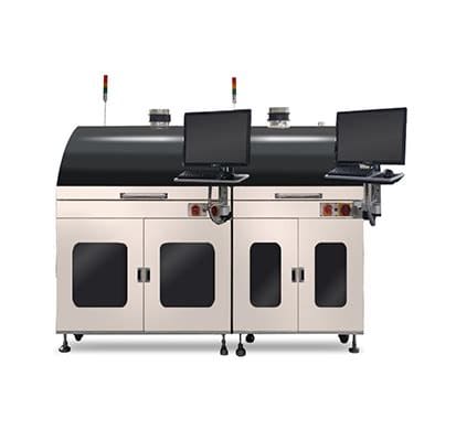
What is Selective Soldering?
Selective soldering is a process used in PCB assembly where specific components or areas of a circuit board are soldered without affecting other parts. It allows for precise application of solder to specific through-hole components, connectors, or pins while leaving adjacent surface mount components untouched.
Selective soldering offers several advantages over wave soldering or manual hand soldering:
- Greater precision and control
- Reduced thermal stress on components
- Ability to solder boards with mixed component types (SMT and through-hole)
- Increased automation and repeatability
- Elimination of masking operations required with wave soldering
How Selective Soldering Works
The selective soldering process typically involves the following steps:
-
The PCB is loaded into a pallet or carrier and secured in place.
-
The assembly moves into position under a solder nozzle. A camera system identifies the component leads or pins to be soldered based on pre-programmed XY coordinates.
-
Flux is applied to the solder points, usually by a small jet or spray. The flux cleans the metal surfaces and helps the solder adhere.
-
The nozzle then applies solder to the specific component leads. Solder is rapidly jetted out in a precise stream. Nozzle geometry, temperature, solder flow rate, and dwell time are carefully controlled.
-
The solder solidifies and forms solder joints as it cools. Joints are formed only where the solder stream contacted the component leads and PCB pads.
-
After soldering, the PCB assembly is cleaned to remove flux residues.
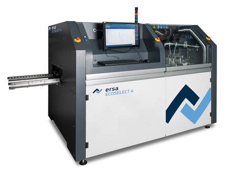
Selective Soldering Equipment and Process Parameters
Solder Nozzles and Tooling
Selective solder nozzles come in various sizes and geometries suited for different component types. Nozzle selection depends on the lead pitch, component density, thermal mass, and required solder joint geometry.
Common nozzle types include:
- Single-point nozzles for soldering individual pins
- Multi-point nozzles with multiple apertures for soldering IC leads or connector pins
- Mini-wave nozzles that create a small turbulent wave for soldering rows of leads
Tooling includes pallets or carriers that hold the PCB stationary and masks that expose only the desired solder points. Proper tooling design is critical for consistent results.
Flux Application
Flux is essential for removing oxides, preventing re-oxidation, and promoting solder wetting. Liquid fluxes are used in selective soldering and can be:
- Alcohol-based for fast evaporation and compatibility with no-clean processes
- Water-soluble for superior oxide removal but requires cleaning after soldering
- Rosin-based for high activity levels
Flux can be applied by:
- Micro-spray nozzles for localized application
- Ultrasonic spray nozzles for fine atomization and uniform coverage
- Foam fluxers that apply flux by direct contact with a foam pad
Flux volume must be sufficient for oxide removal but not excessive to prevent splatter, bridging, or residue-related issues.
Solder Alloy Selection
Tin-Lead (SnPb) solder alloys are commonly used in selective soldering for their ease of processing, good wetting, and reliability. However, lead-free alloys like SAC305 are becoming increasingly common due to RoHS requirements.
Solder alloy selection depends on the PCB’s operating environment, reliability requirements, and compatibility with component finishes. Factors to consider include:
- Melting temperature
- Wetting speed and force
- Mechanical strength of solder joint
- Resistance to thermal cycling and fatigue
- Cost and availability
Process Parameter Optimization
Achieving high-quality solder joints with selective soldering requires careful optimization of process parameters:
- Solder temperature: Typically 40-50°C above alloy melting point for good wetting
- Solder flow rate: Sufficient for filling joints without causing bridging or splatter
- Nozzle dwell time: Long enough for complete joint filling but not excessive
- Nozzle height: Low enough to prevent solder splatter but high enough to avoid nozzle contact
- Preheat settings: To reduce thermal shock and activate flux
- Conveyor speed: Slow enough to allow complete joint filling
Parameter settings vary with PCB design, component types, and solder alloy. Optimization often involves design of experiments (DOE) to determine the most critical parameters and find the optimal settings.
Defect Prevention and Quality Control
Common Selective Soldering Defects
While selective soldering offers quality benefits compared to other processes, defects can still occur if parameters are not properly set or if there are issues with the PCB design or components.
Common defects include:
- Incomplete hole fill: Not enough solder fills the through-hole, often due to insufficient dwell time, low solder temperature, or poor wetting.
- Solder bridges: Excess solder connects adjacent pins or pads, often due to high solder flow, close lead spacing, or excessive flux.
- Solder balls: Small spheres of solder adhere to the PCB surface, often due to solder splatter or excessive dwell time.
- Flux residues: Flux is not fully activated or remains on the board after soldering, often due to low soldering temperature or insufficient cleaning.
- Thermal damage: Sensitive components are damaged by the heat of molten solder, often due to high temperature, long dwell time, or insufficient preheat.
Defect rates with selective soldering are typically below 10 defects per million opportunities (DPMO) when the process is properly optimized.
Design for Selective Soldering
Many selective soldering defects can be prevented through proper PCB design. Guidelines include:
- Providing adequate lead-to-hole clearance (min. 100 μm)
- Avoiding excessive lead-to-lead spacing (min. 0.65 mm)
- Using tear-drop or rounded PCB pad geometry
- Minimizing component thermal mass
- Providing proper spacing between through-hole and SMT components
- Orientation of through-hole components along the direction of travel
- Avoiding obstruction of flux and solder access
Following these guidelines improves manufacturability and reduces the risk of defects.
Quality Control and Inspection
Selective soldering quality is monitored through:
- Visual inspection of solder joints for hole fill, bridging, solder balls, etc.
- X-ray inspection for voids, cracks, or other internal defects
- Cross-sectioning of solder joints to evaluate geometry and microstructure
- Electrical testing for opens, shorts, or resistance issues
- Thermal cycling or mechanical testing for solder joint reliability
Automated optical inspection (AOI) is increasingly used for rapid, consistent detection of visible defects. 3D solder paste inspection (SPI) can measure hole fill and identify insufficient solder volume.
Implementing statistical process control (SPC) and regularly monitoring key process parameters helps identify trends or issues before defects occur.

Benefits and Applications of Selective Soldering
Benefits of Selective Soldering
Selective soldering offers several benefits compared to wave soldering or hand soldering:
- Improved control and precision, reducing defects and rework
- Elimination of masking operations and related costs and waste
- Ability to process PCBs with high component mix and density
- Reduced thermal stress on components
- Faster processing time compared to hand soldering
- Better process monitoring and traceability
These benefits make selective soldering an attractive choice for many PCB assembly applications.
Typical Applications
Selective soldering is commonly used for:
- Assemblies with through-hole components that cannot withstand wave soldering
- Boards with both SMT and through-hole components
- Connectors, pins, or other components with tight lead spacing
- High-reliability aerospace, medical, or military electronics
- Prototyping or low-volume production runs
As component density and complexity increase, selective soldering becomes an increasingly valuable tool for PCB assemblers.

Conclusion
Selective soldering is a versatile and precise process for soldering through-hole components on PCBs. By targeting only specific areas of the board, it enables processing of complex, high-density assemblies.
Achieving high quality and reliability with selective soldering requires careful control of the process parameters, proper PCB design, and regular monitoring and inspection.
As electronics continue to advance, selective soldering will play an increasingly important role in PCB assembly.
Frequently Asked Questions
What are the advantages of selective soldering over wave soldering?
Selective soldering offers several advantages: no masking required, reduced thermal stress, ability to process boards with SMT and through-hole components, and greater precision and control. Wave soldering exposes the entire board to molten solder, requiring masking and potentially causing damage.
Can selective soldering be used with lead-free solder alloys?
Yes, selective soldering is compatible with lead-free alloys like SAC305. The higher melting point and slower wetting of lead-free solders requires higher solder temperature and longer dwell time compared to SnPb solders.
How much flux should be applied during selective soldering?
Flux volume should be enough to effectively remove oxides and promote wetting, typically around 500-1000 μg/in². Too little flux can result in poor hole fill or de-wetting, while too much flux can cause bridging, solder balls, or excessive residues.
What is the typical defect rate with selective soldering?
When the process is properly optimized, selective soldering can achieve defect rates below 10 DPMO (defects per million opportunities). This is lower than typical rates for wave soldering (around 100 DPMO) or hand soldering (500+ DPMO).
How can selective soldering defects be prevented?
Many selective soldering defects can be prevented by proper PCB design (adequate lead-to-hole clearance, lead spacing, pad geometry, etc.), optimization of process parameters (solder temperature, dwell time, flux volume, etc.), and regular monitoring and SPC to identify and correct issues.
No responses yet