Understanding the Basics of PCB Power Distribution Networks
What is a Power Distribution Network?
A power distribution network (PDN) is the system of conductors, planes, and vias that distribute power from the power source to the various components on a PCB. The primary goal of a PDN is to provide a low-impedance path for the current to flow while maintaining a stable voltage level across the board.
The PDN consists of several key elements:
- Power planes
- Ground planes
- Decoupling capacitors
- Vias
- Power traces
The Importance of a Well-Designed PDN
A properly designed PDN is crucial for several reasons:
- Ensures reliable power delivery to all components
- Minimizes voltage drops and fluctuations
- Reduces noise and EMI
- Improves signal integrity
- Prevents ground bounce and voltage sag
Neglecting the PDN design can lead to various issues, such as:
- Intermittent device failures
- Reduced component lifespan
- Increased emissions and susceptibility to external interference
- Degraded signal quality
Designing an Effective PCB Power Distribution Network
Step 1: Determine Power Requirements
The first step in designing a PDN is to determine the power requirements of your PCB. This involves identifying the voltage levels, current draw, and power consumption of each component on the board. Create a power budget table to summarize this information:
| Component | Voltage (V) | Current (mA) | Power (mW) |
|---|---|---|---|
| MCU | 3.3 | 150 | 495 |
| Sensor | 5.0 | 50 | 250 |
| LED | 3.3 | 20 | 66 |
| Total | – | 220 | 811 |
Step 2: Select the Appropriate Power Supply
Based on the power budget, choose a power supply that can deliver the required voltage levels and current. Consider factors such as efficiency, ripple, and regulation when selecting a power supply. Linear regulators and switching regulators are two common options:
| Power Supply Type | Advantages | Disadvantages |
|---|---|---|
| Linear Regulator | – Simple design – Low noise |
– Low efficiency – Heat generation |
| Switching Regulator | – High efficiency – Compact size |
– Higher noise – Complex design |
Step 3: Design Power and Ground Planes
Power and ground planes play a vital role in distributing power evenly across the PCB. Follow these guidelines when designing power and ground planes:
- Use dedicated planes for each voltage level
- Keep power and ground planes close together to minimize inductance
- Avoid splitting planes unnecessarily
- Provide adequate copper coverage for current carrying capacity
- Use solid planes instead of gridded planes for better current distribution
Step 4: Place and Route Power Traces
When placing and routing power traces, consider the following:
- Use wide traces to handle the required current
- Keep power traces as short as possible to minimize resistance and inductance
- Avoid sharp corners and use 45-degree angles for turns
- Separate power traces from sensitive signals to reduce crosstalk
- Use multiple vias for high-current connections
Step 5: Implement Proper Decoupling
Decoupling capacitors are essential for maintaining a stable voltage supply and reducing noise. Follow these best practices for decoupling:
- Place decoupling capacitors close to the power pins of ICs
- Use a combination of bulk, ceramic, and small-value capacitors
- Choose capacitors with low equivalent series resistance (ESR) and equivalent series inductance (ESL)
- Provide adequate land area for capacitor pads
- Use ground vias near decoupling capacitors to minimize loop inductance
Step 6: Optimize Via Placement and Sizing
Vias are used to connect different layers of the PCB and play a crucial role in the PDN. When placing and sizing vias, consider the following:
- Use enough vias to handle the required current
- Place vias close to the power pins of components
- Minimize via inductance by using shorter and wider vias
- Use thermal relief pads for vias in power planes
- Avoid placing vias in high-speed signal paths
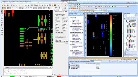
Step 7: Simulate and Verify the PDN Design
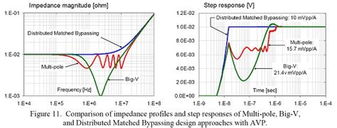
Before finalizing the PCB layout, simulate and verify the PDN design using specialized tools. PDN simulation helps identify potential issues and optimize the design for better performance. Some popular PDN simulation tools include:
- Ansys SIwave
- Cadence Sigrity PowerDC
- Mentor Graphics HyperLynx PI
- Altium Designer Power Distribution Network
Simulation results can help you refine the PDN design by identifying areas for improvement, such as:
- Adjusting plane thickness and spacing
- Optimizing decoupling capacitor placement and values
- Modifying via sizes and locations
- Improving power trace routing
Best Practices for PCB Power Distribution Network Design
To ensure a robust and efficient PDN, follow these best practices:
- Start with a solid power budget and requirements analysis
- Choose appropriate power supplies and regulators
- Use dedicated power and ground planes
- Implement proper decoupling techniques
- Optimize via placement and sizing
- Simulate and verify the PDN design
- Consider the impact of component placement on the PDN
- Use power integrity analysis tools to identify and resolve issues
- Collaborate with the PCB layout team to ensure PDN requirements are met
- Document and communicate PDN design decisions and guidelines

PCB-PDN Design Checklist
Use this checklist to ensure that your PDN design covers all the essential aspects:
- [ ] Power budget and requirements defined
- [ ] Power supply and regulators selected
- [ ] Power and ground planes designed
- [ ] Power traces placed and routed
- [ ] Decoupling capacitors implemented
- [ ] Via placement and sizing optimized
- [ ] PDN design simulated and verified
- [ ] Component placement considered
- [ ] Power integrity analysis performed
- [ ] PDN design documented and communicated
Frequently Asked Questions (FAQ)
1. What is the difference between a power plane and a ground plane?
A power plane is a continuous copper layer that distributes a specific voltage level across the PCB. A ground plane, on the other hand, provides a low-impedance return path for the current. Power and ground planes work together to create a stable and efficient PDN.
2. Why are decoupling capacitors important in PDN design?
Decoupling capacitors are used to provide a local energy storage reservoir for ICs and to filter out high-frequency noise. They help maintain a stable voltage supply and reduce the impact of transient currents, ensuring proper functioning of the components on the PCB.
3. What is the role of vias in a PDN?
Vias are used to connect different layers of the PCB, allowing current to flow between power and ground planes and to the components. Vias play a crucial role in the PDN by providing low-impedance paths for the current and helping to distribute power evenly across the board.
4. How can PDN simulation help improve the design?
PDN simulation tools analyze the power distribution network and provide insights into its performance. They can help identify potential issues, such as voltage drops, impedance mismatches, and resonance peaks. By simulating the PDN, designers can optimize the design for better power delivery, reduced noise, and improved signal integrity.
5. What are some common pitfalls to avoid in PCB-PDN design?
Some common pitfalls to avoid in PCB-PDN design include:
- Neglecting to create a comprehensive power budget
- Failing to use dedicated power and ground planes
- Inadequate decoupling or improper placement of decoupling capacitors
- Ignoring via placement and sizing considerations
- Skipping PDN simulation and verification steps
By understanding and addressing these pitfalls, designers can create more robust and efficient power distribution networks for their PCBs.
Conclusion
A well-designed power distribution network is essential for ensuring the proper functioning, reliability, and performance of a PCB. By understanding the basics of PDN design, following best practices, and using appropriate tools and techniques, designers can create efficient and robust power delivery systems. Remember to start with a solid power budget, use dedicated planes, implement proper decoupling, optimize via placement, and simulate and verify the design. By paying attention to the critical aspects of PCB-PDN design, you can ensure that your PCBs have a stable and reliable power foundation, enabling them to perform at their best.
No responses yet