Introduction to PCB Design and Altium Designer
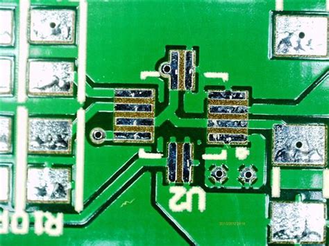
Printed Circuit Boards (PCBs) are the backbone of modern electronics. They provide a platform for components to be mounted and interconnected, enabling complex circuits to be created in a compact and reliable form. Designing a PCB can be a daunting task, especially for those new to the process. However, with the right tools and knowledge, anyone can create professional-quality PCBs.
One of the most popular PCB design tools is Altium Designer. This software package provides a comprehensive set of features for designing and manufacturing PCBs. In this article, we will take you on a journey through the process of creating a schematic in Altium Designer, from concept to completion.
Understanding the Basics of Schematic Design
Before diving into Altium Designer, it’s important to understand the basics of schematic design. A schematic is a graphical representation of an electronic circuit, showing the components and their interconnections. It serves as a blueprint for the PCB layout and is essential for communicating the design intent to others.
Schematic Symbols and Libraries
In a schematic, components are represented by symbols. These symbols are standardized representations of the physical components, making it easy to identify them at a glance. Altium Designer comes with a vast library of pre-made symbols for common components, but you can also create your own symbols if needed.
Nets and Connections
Components in a schematic are connected by nets, which represent the electrical connections between them. Nets are typically named to make it easy to identify their purpose, such as “VCC” for the power supply or “GND” for ground.
Hierarchical Design
For complex designs, it’s often necessary to break the schematic into smaller, more manageable pieces. This is where hierarchical design comes in. With hierarchical design, you can create sub-circuits that are represented by a single symbol in the top-level schematic. This makes the schematic more readable and easier to navigate.

Getting Started with Altium Designer
Now that you have a basic understanding of schematic design, let’s dive into Altium Designer.
Installation and Licensing
The first step is to install Altium Designer on your computer. You can download the software from the Altium website, but you will need a valid license to use it. Altium offers a variety of licensing options, including perpetual licenses and subscription-based plans.
Creating a New Project
Once you have Altium Designer installed and licensed, you can create a new project. To do this, click on the “File” menu and select “New Project”. Give your project a name and choose a location to save it.
The Altium Designer Interface
The Altium Designer interface can be overwhelming at first, but it’s actually quite intuitive once you get used to it. The main window is divided into several panels, including the schematic editor, the PCB editor, and the libraries panel.

Creating a Schematic in Altium Designer
Now that you’re familiar with the Altium Designer interface, let’s start creating a schematic.
Adding Components
The first step in creating a schematic is to add components. To do this, open the libraries panel and browse for the components you need. You can also search for components by name or part number.
Once you’ve found the component you want, simply drag and drop it onto the schematic editor. You can then position the component where you want it and rotate it if necessary.
Connecting Components
After adding components, you need to connect them with nets. To do this, simply click on the pin of one component and drag a wire to the pin of another component. You can also use the “Place Wire” tool to create nets automatically.
When connecting components, it’s important to pay attention to the net names. Give your nets meaningful names that describe their purpose, such as “VCC” for the power supply or “DATA” for a data bus.
Adding Power and Ground Symbols
Most schematics will require power and ground symbols to represent the power supply and ground connections. Altium Designer comes with pre-made symbols for these, which you can find in the libraries panel.
To add a power or ground symbol, simply drag and drop it onto the schematic editor. You can then connect it to the appropriate nets using wires.
Annotating Components
As you add components to your schematic, you may notice that they have generic designators like “R?” or “C?”. These are placeholder designators that need to be updated with unique identifiers.
To annotate your components, select them all and then click on the “Tools” menu and select “Annotate”. Choose the annotation options you want and click “OK”. Altium Designer will then assign unique designators to each component.
Adding Net Labels
Net labels are used to give names to nets that are not connected to a pin. They are useful for clarifying the purpose of a net or for connecting nets across multiple pages of a schematic.
To add a net label, simply click on the “Place Net Label” tool and then click on the net you want to label. Type in the name of the net and press “Enter”.
Creating a Bill of Materials (BOM)
A Bill of Materials (BOM) is a list of all the components used in a design, along with their quantities and other relevant information. Altium Designer can automatically generate a BOM from your schematic, making it easy to keep track of your components.
To generate a BOM, click on the “Reports” menu and select “Bill of Materials”. Choose the options you want and click “Generate”. Altium Designer will then create a spreadsheet with all the components used in your design.

Advanced Schematic Design Techniques
Once you’ve mastered the basics of schematic design in Altium Designer, there are several advanced techniques you can use to improve your designs.
Using Busses
Busses are used to simplify the representation of multiple nets that are related, such as a data bus or an address bus. Instead of drawing individual wires for each net, you can use a bus to represent them all with a single line.
To create a bus, simply draw a line using the “Place Bus” tool and then add bus entries to represent the individual nets. You can then connect the bus entries to components using wires.
Creating Hierarchical Blocks
Hierarchical blocks are used to simplify complex schematics by breaking them down into smaller, more manageable pieces. Each block represents a sub-circuit that can be reused in other parts of the design.
To create a hierarchical block, first create the sub-circuit in a separate schematic file. Then, in the main schematic, add a “Sheet Symbol” to represent the sub-circuit. You can then connect the sheet symbol to other components using ports.
Using Design Rules
Design rules are used to enforce consistency and ensure that your schematic meets certain standards. Altium Designer comes with a set of built-in design rules, but you can also create your own.
To access the design rules, click on the “Tools” menu and select “Design Rule Check”. From here, you can enable or disable specific rules and set their parameters.
Simulating Your Design
Simulation is a powerful tool for verifying the behavior of your circuit before you build it. Altium Designer comes with a built-in simulator that can be used to test your design.
To simulate your design, first set up the simulation parameters in the “Simulation Setup” dialog. Then, add probes to the nets you want to monitor and run the simulation. Altium Designer will then generate waveforms that show the behavior of your circuit over time.
Best Practices for Schematic Design
To ensure that your schematics are clear, accurate, and easy to understand, follow these best practices:
Keep It Simple
Avoid clutter and unnecessary complexity in your schematics. Use hierarchical design techniques to break down complex circuits into smaller, more manageable pieces.
Use Consistent Naming Conventions
Use consistent naming conventions for your components, nets, and other elements. This will make your schematics easier to read and understand.
Follow Industry Standards
Follow industry standards for schematic symbols, net names, and other elements. This will make your schematics more readable and ensure that they can be easily understood by others.
Document Your Design
Include comments and notes in your schematics to clarify the purpose of each element and explain any design decisions you made. This will make it easier for others to understand and maintain your design in the future.
Review and Verify Your Design
Before finalizing your schematic, review it carefully to ensure that it is accurate and complete. Use the design rule checks and simulation tools to verify that your design behaves as expected.
Frequently Asked Questions (FAQ)
- What is the difference between a schematic and a PCB layout?
-
A schematic is a graphical representation of an electronic circuit, showing the components and their interconnections. A PCB layout, on the other hand, is a physical representation of the circuit, showing the actual placement and routing of components on a printed circuit board.
-
Can I create my own component symbols in Altium Designer?
-
Yes, you can create your own component symbols in Altium Designer. To do this, open the library editor and create a new symbol. You can then add pins, graphics, and other elements to create a custom symbol.
-
What is the purpose of a net label in a schematic?
-
A net label is used to give a name to a net that is not connected to a pin. This can be useful for clarifying the purpose of a net or for connecting nets across multiple pages of a schematic.
-
How do I generate a Bill of Materials (BOM) in Altium Designer?
-
To generate a BOM in Altium Designer, click on the “Reports” menu and select “Bill of Materials”. Choose the options you want and click “Generate”. Altium Designer will then create a spreadsheet with all the components used in your design.
-
What is the purpose of design rules in Altium Designer?
- Design rules are used to enforce consistency and ensure that your schematic meets certain standards. They can be used to check for errors, ensure that components are properly connected, and enforce naming conventions.
Conclusion
Creating a schematic in Altium Designer is a key skill for anyone involved in PCB design. By following the steps outlined in this article, you can create professional-quality schematics that are clear, accurate, and easy to understand.
Remember to keep your schematics simple, use consistent naming conventions, follow industry standards, and document your design. By doing so, you’ll be well on your way to creating a thousand PCBs and beyond.
| Step | Description |
|---|---|
| 1 | Install Altium Designer and create a new project |
| 2 | Add components to your schematic |
| 3 | Connect components using nets and buses |
| 4 | Add power and ground symbols |
| 5 | Annotate components and add net labels |
| 6 | Generate a Bill of Materials (BOM) |
| 7 | Use advanced techniques like hierarchical design and simulation |
| 8 | Follow best practices for schematic design |
With practice and patience, anyone can master the art of schematic design in Altium Designer. So what are you waiting for? Start your journey to a thousand PCBs today!

No responses yet