Introduction to SAP-PCB Technology
Semi-Additive Process (SAP) PCB, also known as SAP-PCB, is an advanced manufacturing technique for printed circuit boards that offers several advantages over traditional PCB production methods. This technology enables the creation of high-density interconnect (HDI) PCBs with fine features, improved electrical performance, and enhanced reliability.
Key Features of SAP-PCB
- Fine line and space: SAP-PCB allows for the creation of traces and spaces as small as 25 microns, enabling higher routing density and more compact designs.
- Thin copper foils: The process uses thin copper foils, typically ranging from 5 to 15 microns, which contributes to improved signal integrity and reduced signal loss.
- Reduced via size: SAP-PCB technology enables the creation of smaller vias, leading to higher via density and more efficient use of board space.
- Improved impedance control: The precise control over trace geometry and dielectric thickness in SAP-PCB results in better impedance control, which is critical for high-speed applications.
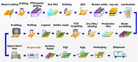
The SAP-PCB Manufacturing Process
The SAP-PCB manufacturing process involves several key steps that distinguish it from conventional PCB production methods. Here’s an overview of the process:
- Substrate preparation: A thin copper foil is laminated onto a dielectric substrate, such as FR-4 or polyimide.
- Resist application: A photoresist layer is applied to the copper foil and patterned using photolithography to define the desired circuit layout.
- Copper plating: Additional copper is electroplated onto the exposed areas of the copper foil, building up the thickness of the traces and vias.
- Resist removal: The photoresist is stripped away, leaving behind the plated copper traces and vias.
- Etching: The thin copper foil is etched away, leaving only the plated copper features on the substrate.
- Multilayer lamination: For multilayer SAP-PCBs, additional dielectric layers and copper foils are laminated together, and the process is repeated for each layer.
Advantages of SAP-PCB Technology
SAP-PCB technology offers several advantages over traditional PCB manufacturing methods:
- Higher density: The fine feature sizes and reduced via dimensions enable higher routing density, allowing for more compact and complex designs.
- Improved signal integrity: The thin copper foils and precise trace geometry control contribute to better signal integrity and reduced signal loss, making SAP-PCB ideal for high-speed applications.
- Enhanced reliability: The use of electroplated copper results in a more uniform and consistent trace thickness, improving the overall reliability of the PCB.
- Cost-effective: While the SAP-PCB process may have higher initial setup costs, it can be more cost-effective in the long run, particularly for high-volume production runs.

Applications of SAP-PCB
SAP-PCB technology is well-suited for a wide range of applications that require high-density interconnects, improved signal integrity, and enhanced reliability. Some common applications include:
- High-speed digital devices
- Telecommunications equipment
- Automotive electronics
- Medical devices
- Aerospace and defense systems
- Consumer electronics
Top 5 Questions Regarding SAP-PCB Stack
1. What is the typical stack-up for a SAP-PCB?
A typical SAP-PCB stack-up consists of alternating layers of dielectric substrate and copper. The number of layers can vary depending on the complexity of the design and the application requirements. Here’s an example of a 6-layer SAP-PCB stack-up:
| Layer | Material | Thickness (μm) |
|---|---|---|
| 1 | Copper | 15 |
| – | Dielectric | 100 |
| 2 | Copper | 15 |
| – | Dielectric | 200 |
| 3 | Copper | 15 |
| – | Dielectric | 200 |
| 4 | Copper | 15 |
| – | Dielectric | 200 |
| 5 | Copper | 15 |
| – | Dielectric | 100 |
| 6 | Copper | 15 |
2. How does the dielectric material choice affect the SAP-PCB stack?
The choice of dielectric material is critical in SAP-PCB stack design, as it directly impacts the electrical performance and reliability of the PCB. The most common dielectric materials used in SAP-PCB are FR-4 and polyimide.
- FR-4: A glass-reinforced epoxy laminate that offers good mechanical strength, thermal stability, and electrical insulation properties. FR-4 is widely used in PCB manufacturing and is a cost-effective option for many applications.
- Polyimide: A high-performance polymer that offers excellent thermal stability, chemical resistance, and electrical insulation properties. Polyimide is often used in high-reliability applications that require superior performance under demanding conditions.
The dielectric material choice affects the following aspects of the SAP-PCB stack:
- Dielectric constant: The dielectric constant (Dk) determines the speed at which signals propagate through the material. A lower Dk results in faster signal propagation and reduced signal delay.
- Dissipation factor: The dissipation factor (Df) represents the amount of energy lost as heat when an electrical signal passes through the dielectric. A lower Df results in less signal loss and improved signal integrity.
- Thermal performance: The thermal conductivity and coefficient of thermal expansion (CTE) of the dielectric material influence the PCB’s ability to dissipate heat and maintain structural integrity under temperature fluctuations.
3. What are the considerations for designing vias in a SAP-PCB stack?
Vias are essential components in a SAP-PCB stack, as they provide electrical connections between layers. When designing vias in a SAP-PCB stack, several factors must be considered:
- Via size: SAP-PCB technology enables the creation of smaller vias compared to traditional PCB manufacturing methods. The via size should be optimized based on the design requirements, such as routing density and signal integrity.
- Via type: There are several types of vias used in SAP-PCB, including through-hole vias, blind vias, and buried vias. The choice of via type depends on the layer interconnections required and the overall design complexity.
- Via placement: The placement of vias in a SAP-PCB stack should be carefully considered to minimize signal reflections, crosstalk, and electromagnetic interference (EMI). Vias should be placed away from critical signal traces and spaced appropriately to maintain signal integrity.
- Via stubs: Via stubs are the unused portions of a via that can cause signal reflections and degrade signal quality. In high-speed designs, via stubs should be minimized or eliminated using techniques such as back-drilling or blind via technology.
4. How does the SAP-PCB stack affect signal integrity?
The SAP-PCB stack has a significant impact on signal integrity, particularly in high-speed applications. Several factors contribute to the signal integrity performance of a SAP-PCB stack:
- Trace geometry: The width, thickness, and spacing of traces in a SAP-PCB stack directly influence signal integrity. Thinner traces and smaller spaces can lead to increased crosstalk and signal reflections, while wider traces and larger spaces can improve signal quality.
- Dielectric properties: The dielectric constant (Dk) and dissipation factor (Df) of the dielectric material used in the SAP-PCB stack affect signal propagation speed and loss. A lower Dk and Df generally result in better signal integrity.
- Impedance control: Maintaining consistent impedance throughout the SAP-PCB stack is crucial for preserving signal integrity. This is achieved by carefully controlling the trace geometry and dielectric thickness, as well as using appropriate termination techniques.
- Via design: As mentioned earlier, via size, type, placement, and stub minimization are critical factors in maintaining signal integrity in a SAP-PCB stack.
To optimize signal integrity in a SAP-PCB stack, designers often use simulation tools and adhere to established design guidelines, such as controlled impedance routing, proper signal trace spacing, and appropriate via design practices.
5. What are the challenges in manufacturing SAP-PCB stacks?
While SAP-PCB technology offers numerous advantages, there are several challenges associated with manufacturing SAP-PCB stacks:
- Process control: The SAP-PCB manufacturing process requires precise control over various parameters, such as copper plating thickness, etching uniformity, and dielectric layer alignment. Maintaining consistent process control can be challenging, particularly for high-volume production runs.
- Equipment requirements: SAP-PCB manufacturing requires specialized equipment, such as high-resolution photolithography systems, advanced electroplating tools, and precise etching machines. The cost and availability of this equipment can be a barrier for some PCB manufacturers.
- Material selection: Choosing the appropriate dielectric materials and copper foils for SAP-PCB stacks can be challenging, as they must meet specific requirements for electrical performance, thermal stability, and manufacturability. The availability and cost of these materials can also be a concern.
- Design complexity: As SAP-PCB technology enables higher routing density and finer features, the complexity of PCB designs can increase significantly. This complexity can lead to challenges in design verification, signal integrity analysis, and manufacturability assessment.
- Testing and inspection: Ensuring the quality and reliability of SAP-PCB stacks requires advanced testing and inspection techniques, such as automated optical inspection (AOI), X-ray inspection, and electrical testing. These techniques can be time-consuming and costly, but are essential for identifying and addressing any manufacturing defects or performance issues.
To overcome these challenges, PCB manufacturers and designers must work closely together, leveraging advanced design tools, process optimization techniques, and quality control measures to ensure the successful production of high-quality SAP-PCB stacks.
Conclusion
SAP-PCB technology is a powerful solution for creating high-density, high-performance printed circuit boards that meet the demands of modern electronic devices. By understanding the key aspects of SAP-PCB stack design, including dielectric material selection, via design considerations, and signal integrity optimization, designers can harness the full potential of this advanced manufacturing process.
While there are challenges associated with manufacturing SAP-PCB stacks, the benefits of this technology – including higher routing density, improved signal integrity, and enhanced reliability – make it an increasingly popular choice for a wide range of applications. As the electronics industry continues to push the boundaries of performance and miniaturization, SAP-PCB technology is poised to play a crucial role in enabling the next generation of innovative devices.
No responses yet