Understanding PCB Height and Its Importance
Printed Circuit Board (PCB) height is a crucial factor to consider when designing and manufacturing electronic devices. The height of a PCB refers to the distance between the top and bottom surfaces of the board, including all components and connectors. It is essential to adhere to PCB height restrictions to ensure proper functionality, compatibility, and reliability of the final product.
Why PCB Height Matters
-
Compatibility: PCB height restrictions ensure that the board fits properly within the designated enclosure or device. Exceeding the specified height can lead to issues with assembly and integration.
-
Clearance: Adequate clearance between the PCB and other components, such as heatsinks or mechanical parts, is necessary to avoid short circuits and physical damage.
-
Thermal Management: The height of components on the PCB can affect heat dissipation. Proper height management helps in maintaining optimal thermal performance.
-
Signal Integrity: The height of certain components, such as connectors or tall components, can impact signal integrity. Adhering to height restrictions minimizes signal distortion and interference.
Factors Affecting PCB Height
Several factors contribute to the overall height of a PCB:
-
Component Height: The height of individual components, such as integrated circuits (ICs), capacitors, and resistors, plays a significant role in determining the total PCB height.
-
Connector Height: Connectors, such as USB ports, HDMI connectors, or power jacks, can add substantial height to the PCB.
-
Solder Joint Height: The height of solder joints, especially for through-hole components, contributes to the overall PCB height.
-
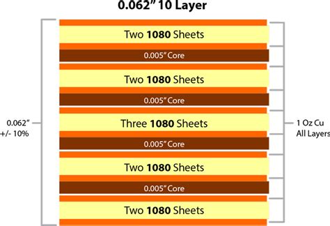
PCB Thickness: The thickness of the PCB substrate itself, which can vary based on the number of layers and material choice, affects the total height.
PCB Height Restriction Standards
Various industry standards and guidelines provide recommendations for PCB height restrictions. Some common standards include:
| Standard | Description |
|---|---|
| IPC-2221 | Generic Standard on Printed Board Design |
| IPC-2223 | Sectional Design Standard for Flexible Printed Boards |
| IPC-7351 | Generic Requirements for Surface Mount Design and Land Pattern |
| JEDEC MO-256 | Chip Scale Package (CSP) Design Guidelines |
These standards offer guidance on recommended heights for different components and provide best practices for PCB design and manufacturing.

Designing PCBs with Height Restrictions in Mind
To effectively design PCBs while adhering to height restrictions, consider the following tips:
1. Choose Low-Profile Components
When possible, select components with low-profile packages to minimize the overall height of the PCB. Some examples include:
- Flat pack ICs instead of dual in-line packages (DIP)
- Surface mount devices (SMD) instead of through-hole components
- Low-profile connectors
2. Optimize Component Placement
Strategic component placement can help in managing PCB height:
- Place taller components, such as connectors or large capacitors, near the edges of the board to avoid interference with other components.
- Group components with similar heights together to create a more uniform height distribution across the PCB.
3. Consider Using Blind and Buried Vias
Blind and buried vias can help reduce the overall height of the PCB by allowing connections between inner layers without extending to the top or bottom surfaces. This technique is particularly useful for high-density designs with limited space.
4. Use Appropriate Solder Joint Heights
Ensure that the solder joint heights for through-hole components are within the specified limits. Excessive solder joints can cause issues with height clearance and affect the reliability of the connections.
5. Collaborate with PCB Manufacturers
Engage with PCB manufacturers early in the design process to discuss height restrictions and manufacturing capabilities. They can provide valuable insights and recommendations based on their expertise and experience.
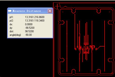
PCB Height Measurement Techniques
Accurate measurement of PCB height is crucial for ensuring compliance with height restrictions. Some common measurement techniques include:
-
Caliper Measurement: Using digital or vernier calipers to measure the distance between the top and bottom surfaces of the PCB at various points.
-
3D Scanning: Employing 3D scanning technologies, such as structured light scanning or laser scanning, to create a digital model of the PCB and measure its height accurately.
-
Cross-Sectional Analysis: Cutting a cross-section of the PCB and examining it under a microscope to measure the height of individual components and layers.
-
Automated Optical Inspection (AOI): Using AOI systems to capture high-resolution images of the PCB and measure heights using image processing algorithms.
Frequently Asked Questions (FAQ)
-
Q: What happens if a PCB exceeds the specified height restrictions?
A: If a PCB exceeds the specified height restrictions, it may not fit properly within the intended enclosure or device. This can lead to assembly issues, interference with other components, and potential damage to the PCB or surrounding parts. -
Q: Can PCB height restrictions be modified during the design process?
A: In some cases, PCB height restrictions can be modified if the design allows for it and if the changes do not compromise the functionality or reliability of the device. However, it is essential to consult with the relevant stakeholders, such as mechanical engineers or product managers, before making any significant changes. -
Q: How can I ensure that my PCB design meets the specified height restrictions?
A: To ensure compliance with height restrictions, follow best practices such as choosing low-profile components, optimizing component placement, and considering advanced manufacturing techniques like blind and buried vias. Additionally, collaborate with PCB manufacturers and use appropriate measurement techniques to verify the height of your PCB. -
Q: Are there any software tools that can help in managing PCB height during the design phase?
A: Yes, many PCB design software packages include tools for managing and analyzing PCB height. These tools can help in visualizing component heights, detecting potential height violations, and generating 3D models of the PCB for accurate measurements. -
Q: What should I do if I encounter a height restriction violation during the PCB manufacturing process?
A: If a height restriction violation is identified during manufacturing, the first step is to communicate with the PCB manufacturer to assess the severity of the issue. In some cases, minor adjustments to the design or selective assembly techniques may resolve the problem. However, if the violation is significant, it may require a redesign of the affected area or even the entire PCB.
Conclusion
PCB height restrictions play a vital role in ensuring the proper functionality, compatibility, and reliability of electronic devices. By understanding the factors that affect PCB height and following best practices for design and manufacturing, engineers can successfully navigate height constraints and create PCBs that meet the required specifications.
Effective communication and collaboration among design teams, mechanical engineers, and PCB manufacturers are essential for managing PCB height throughout the product development lifecycle. By staying informed about industry standards, utilizing appropriate measurement techniques, and leveraging the expertise of professionals, companies can overcome the challenges associated with PCB height restrictions and deliver high-quality electronic products to market.
No responses yet