Introduction to Rigid-flex PCBs
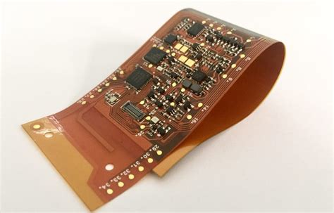
Rigid-Flex PCBs are a unique type of printed circuit board that combines rigid and flexible substrates into a single circuit board. This allows the PCB to be bent and folded into various shapes to fit into tight spaces or movable parts, while still providing the stability and durability of a rigid PCB in other areas.
Rigid-Flex PCBs offer several advantages over traditional rigid PCBs, including:
- Reduced size and weight
- Increased reliability
- Improved signal integrity
- Greater design flexibility
- Simplified assembly
These benefits make Rigid-Flex PCBs ideal for a wide range of applications, particularly in industries where space is limited or the PCB needs to move or flex, such as:
- Aerospace and defense
- Medical devices
- Automotive electronics
- Consumer electronics
- Industrial automation
In this article, we will explore the Rigid-Flex PCB manufacturing process in detail, including the materials and methods used, design considerations, and testing and inspection procedures. We will also discuss some of the key applications of Rigid-Flex PCBs and answer some frequently asked questions about this technology.
Rigid-Flex PCB Manufacturing Process
The Rigid-Flex PCB manufacturing process involves several steps, each of which must be carefully controlled to ensure the highest quality and reliability of the finished product. Here is an overview of the main steps involved:
1. Material Selection
The first step in the Rigid-Flex PCB manufacturing process is to select the appropriate materials for the job. This includes the base material, copper foil, coverlay, adhesives, and other components.
The base material is typically a flexible polyimide film, such as Kapton or Pyralux. This material is chosen for its excellent electrical, thermal, and mechanical properties, as well as its ability to withstand repeated flexing without breaking or degrading.
The copper foil used in Rigid-Flex PCBs is usually a rolled annealed (RA) copper, which is softer and more ductile than the electrodeposited (ED) copper used in rigid PCBs. This allows the copper to bend and flex without cracking or breaking.
The coverlay is a protective layer that is applied over the copper traces to insulate and protect them from damage. It is typically made of a polyimide film with an adhesive backing.
Other materials used in Rigid-Flex PCBs include adhesives for bonding the layers together, stiffeners for added support in rigid areas, and plated through-holes (PTHs) for connecting the layers electrically.
2. Design and Layout
The next step is to design and lay out the circuit board using specialized CAD software. This involves creating a schematic diagram of the circuit, selecting the appropriate components and materials, and laying out the copper traces and other features on the board.
Rigid-Flex PCB Design requires careful consideration of several factors, including:
- Bend radius: The minimum bend radius that the flexible portions of the PCB can withstand without damaging the copper traces or other components.
- Stiffener placement: The location and size of the stiffeners used to support the rigid portions of the PCB.
- Coverlay openings: The size and location of the openings in the coverlay to allow access to the copper traces for soldering or other connections.
- Copper balancing: Ensuring that the copper is evenly distributed across the layers to prevent warping or other issues during manufacturing.
3. Lamination
Once the design is complete, the next step is to laminate the layers together to form the basic structure of the Rigid-Flex PCB. This involves stacking the flexible and rigid substrates in the appropriate order, with adhesive layers in between, and pressing them together under heat and pressure.
The lamination process typically involves several steps:
- Inner layer lamination: The flexible layers are laminated together first, with the copper foil and coverlay in place.
- Drilling: Holes are drilled through the laminated stack to create vias and other features.
- Plating: The holes are plated with copper to create electrical connections between the layers.
- Outer layer lamination: The rigid layers are then laminated onto the flexible stack, with stiffeners in place to support the rigid areas.
4. Etching and Plating
After lamination, the copper on the outer layers of the PCB is etched away to create the desired circuit pattern. This is typically done using a photolithographic process, where a photoresist is applied to the copper and exposed to light through a patterned mask. The unexposed areas are then etched away using a chemical solution, leaving behind the copper traces.
The etched board is then plated with additional copper to build up the thickness of the traces and improve their conductivity. This is typically done using an electroplating process, where the board is immersed in a copper sulfate solution and an electrical current is applied to deposit the copper onto the traces.
5. Solder Mask and Silkscreen
After etching and plating, a solder mask is applied to the PCB to protect the copper traces from oxidation and prevent solder bridging during assembly. The solder mask is typically a green or black epoxy-based material that is screen printed onto the board and cured under UV light.
A silkscreen layer is then applied on top of the solder mask to add labels, logos, and other markings to the PCB. This is typically done using a white or yellow epoxy ink that is screen printed onto the board and cured.
6. Cutting and Profiling
The final step in the Rigid-Flex PCB manufacturing process is to cut and profile the board to its final shape and size. This is typically done using a computer-controlled routing machine or laser cutter, which can accurately cut the board to the desired dimensions and create any necessary cutouts or openings.
The profiled board is then inspected and tested to ensure that it meets all of the required specifications and performance criteria. This may involve visual inspection, electrical testing, and other quality control measures.

Rigid-Flex PCB Design Considerations
Designing a Rigid-Flex PCB requires careful consideration of several key factors to ensure optimal performance and reliability. Here are some of the main design considerations to keep in mind:
Bend Radius
The bend radius is the minimum radius that the flexible portions of the PCB can be bent without damaging the copper traces or other components. This is typically determined by the thickness and material properties of the flexible substrate and the copper foil.
As a general rule, the minimum bend radius should be at least 10 times the total thickness of the flexible layers. For example, if the total thickness of the flexible layers is 0.2mm, the minimum bend radius should be at least 2mm.
Stiffener Placement
Stiffeners are used to provide support and rigidity to the rigid portions of the Rigid-Flex PCB. They are typically made of a rigid material, such as FR-4, and are laminated onto the flexible layers in the appropriate locations.
The placement and size of the stiffeners is critical to ensuring the overall stability and reliability of the PCB. They should be placed in areas where the PCB needs to be rigid, such as connectors or mounting points, and should be sized appropriately to provide adequate support without adding unnecessary weight or bulk.
Coverlay Openings
The coverlay is a protective layer that is applied over the copper traces on the flexible layers of the PCB. It is typically made of a polyimide film with an adhesive backing, and is used to insulate and protect the copper from damage.
Coverlay openings are used to allow access to the copper traces for soldering or other connections. They should be sized and positioned appropriately to ensure that the connections can be made reliably without damaging the coverlay or exposing the copper to potential damage.
Copper Balancing
Copper balancing is the process of ensuring that the copper is evenly distributed across the layers of the Rigid-Flex PCB. This is important to prevent warping or other issues during manufacturing, as well as to ensure optimal electrical performance.
Copper balancing typically involves adding copper pours or other features to the non-signal layers of the PCB to balance out the copper distribution. This can be done using specialized CAD tools that can analyze the copper distribution and suggest appropriate balancing features.

Rigid-Flex PCB Materials
The materials used in Rigid-Flex PCBs are critical to their performance and reliability. Here are some of the main materials used:
Base Material
The base material is the flexible substrate that forms the foundation of the Rigid-Flex PCB. It is typically made of a polyimide film, such as Kapton or Pyralux, which offers excellent electrical, thermal, and mechanical properties.
Polyimide films are chosen for their ability to withstand repeated flexing without breaking or degrading, as well as their high temperature resistance and low dielectric constant.
Copper Foil
The copper foil used in Rigid-Flex PCBs is typically a rolled annealed (RA) copper, which is softer and more ductile than the electrodeposited (ED) copper used in rigid PCBs. This allows the copper to bend and flex without cracking or breaking.
The thickness of the copper foil is typically between 18-70μm, depending on the specific requirements of the application. Thinner copper foil is more flexible but has higher electrical resistance, while thicker copper foil is less flexible but has lower electrical resistance.
Coverlay
The coverlay is a protective layer that is applied over the copper traces to insulate and protect them from damage. It is typically made of a polyimide film with an adhesive backing, and is available in various thicknesses and colors.
The coverlay is typically applied using a lamination process, where it is pressed onto the flexible layers under heat and pressure. Coverlay openings are then created to allow access to the copper traces for soldering or other connections.
Adhesives
Adhesives are used to bond the various layers of the Rigid-Flex PCB together, including the flexible and rigid substrates, copper foil, and coverlay. The choice of adhesive is critical to ensuring reliable bonding and preventing delamination or other issues.
The most common types of adhesives used in Rigid-Flex PCBs are epoxy-based adhesives, which offer excellent strength and durability. Acrylic-based adhesives are also used in some applications, particularly where flexibility is a key requirement.
Stiffeners
Stiffeners are used to provide support and rigidity to the rigid portions of the Rigid-Flex PCB. They are typically made of a rigid material, such as FR-4, and are laminated onto the flexible layers in the appropriate locations.
The choice of stiffener material and thickness depends on the specific requirements of the application, such as the required level of rigidity and the weight and size constraints of the PCB.

Rigid-Flex PCB Testing and Inspection
Testing and inspection are critical steps in the Rigid-Flex PCB manufacturing process to ensure the highest quality and reliability of the finished product. Here are some of the main testing and inspection procedures used:
Visual Inspection
Visual inspection is the first step in the testing and inspection process, and involves examining the PCB for any visible defects or anomalies, such as scratches, dents, or discoloration.
Visual inspection is typically done using a microscope or other magnification device, and may also involve the use of automated optical inspection (AOI) equipment to identify defects more quickly and accurately.
Electrical Testing
Electrical testing is used to verify the electrical performance and functionality of the Rigid-Flex PCB. This may involve testing for continuity, insulation resistance, and other electrical properties using specialized test equipment.
Electrical testing may also involve functional testing, where the PCB is connected to a test system and operated under various conditions to verify that it performs as intended.
Mechanical Testing
Mechanical testing is used to verify the mechanical performance and reliability of the Rigid-Flex PCB, particularly in terms of its ability to withstand repeated flexing and bending.
Mechanical testing may involve subjecting the PCB to various types of stress, such as bending, twisting, or vibration, and measuring its performance and durability over time.
Environmental Testing
Environmental testing is used to verify the performance and reliability of the Rigid-Flex PCB under various environmental conditions, such as temperature, humidity, and altitude.
Environmental testing may involve subjecting the PCB to various types of environmental stress, such as thermal cycling, moisture exposure, or altitude testing, and measuring its performance and reliability over time.
Applications of Rigid-Flex PCBs
Rigid-Flex PCBs are used in a wide range of applications across various industries, particularly where space is limited or the PCB needs to move or flex. Here are some of the main applications of Rigid-Flex PCBs:
Aerospace and Defense
Rigid-Flex PCBs are widely used in aerospace and defense applications, where size, weight, and reliability are critical factors. Examples include:
- Avionics systems
- Missile guidance systems
- Satellite communications equipment
- Unmanned aerial vehicles (UAVs)
Medical Devices
Rigid-Flex PCBs are also used in a variety of medical devices, particularly where the PCB needs to fit into a small or irregularly shaped space. Examples include:
- Wearable medical devices
- Implantable medical devices
- Surgical instruments
- Diagnostic equipment
Automotive Electronics
Rigid-Flex PCBs are used in various automotive electronics applications, particularly where the PCB needs to withstand harsh environmental conditions and vibration. Examples include:
- Engine control modules
- Transmission control modules
- Infotainment systems
- Advanced driver assistance systems (ADAS)
Consumer Electronics
Rigid-Flex PCBs are used in a variety of consumer electronics applications, particularly where the PCB needs to fit into a small or thin form factor. Examples include:
- Smartphones
- Tablets
- Wearable devices
- Cameras
Industrial Automation
Rigid-Flex PCBs are used in various industrial automation applications, particularly where the PCB needs to withstand harsh environmental conditions and vibration. Examples include:
- Robotics
- Automated manufacturing equipment
- Process control systems
- Sensors and actuators
Frequently Asked Questions
Q: What is the difference between a Rigid PCB and a Rigid-Flex PCB?
A: A Rigid PCB is a traditional printed circuit board that is made entirely of rigid materials, such as FR-4. A Rigid-Flex PCB, on the other hand, combines rigid and flexible substrates into a single circuit board, allowing it to bend and flex in certain areas while still providing the stability and durability of a rigid PCB in other areas.
Q: What are the advantages of using a Rigid-Flex PCB?
A: Rigid-Flex PCBs offer several advantages over traditional rigid PCBs, including reduced size and weight, increased reliability, improved signal integrity, greater design flexibility, and simplified assembly.
Q: What materials are used in Rigid-Flex PCBs?
A: The main materials used in Rigid-Flex PCBs include polyimide films for the flexible substrate, rolled annealed copper foil for the conductive layers, coverlay for insulation and protection, adhesives for bonding the layers together, and stiffeners for added support in rigid areas.
Q: What are some of the key applications of Rigid-Flex PCBs?
A: Rigid-Flex PCBs are used in a wide range of applications across various industries, including aerospace and defense, medical devices, automotive electronics, consumer electronics, and industrial automation.
Q: What are some of the key design considerations for Rigid-Flex PCBs?
A: Some of the key design considerations for Rigid-Flex PCBs include bend radius, stiffener placement, coverlay openings, and copper balancing. It is important to carefully consider these factors to ensure optimal performance and reliability of the PCB.
Conclusion
Rigid-Flex PCBs offer a unique combination of flexibility and durability that makes them ideal for a wide range of applications across various industries. By combining rigid and flexible substrates into a single circuit board, Rigid-Flex PCBs can reduce size and weight, increase reliability, improve signal integrity, and simplify assembly.
The Rigid-Flex PCB manufacturing process involves several key steps, including material selection, design and layout, lamination, etching and plating, solder mask and silkscreen application, and cutting and profiling. Each of these steps must be carefully controlled to ensure the highest quality and reliability of the finished product.
When designing a Rigid-Flex PCB, it is important to carefully consider several key factors, including bend radius, stiffener placement, coverlay openings, and copper balancing. By taking these factors into account, designers can ensure optimal performance and reliability of the PCB in the intended application.
Rigid-Flex PCBs are used in a wide range of applications, including aerospace and defense, medical devices, automotive electronics, consumer electronics, and industrial automation. As technology continues to advance and the demand for smaller, lighter, and more reliable electronic devices grows, the use of Rigid-Flex PCBs is likely to increase in the coming years.
No responses yet