Introduction
Radio Frequency (RF) power supplies are essential components in various applications, including telecommunications, broadcasting, and industrial processes. Designing and laying out an efficient and reliable RF power supply requires careful consideration of several factors, such as power requirements, frequency range, and environmental conditions. This comprehensive guide aims to provide a detailed overview of RF power supply design and layout, covering key aspects such as component selection, circuit topology, PCB layout, and troubleshooting.
Understanding RF Power Supply Fundamentals
What is an RF Power Supply?
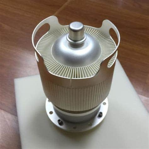
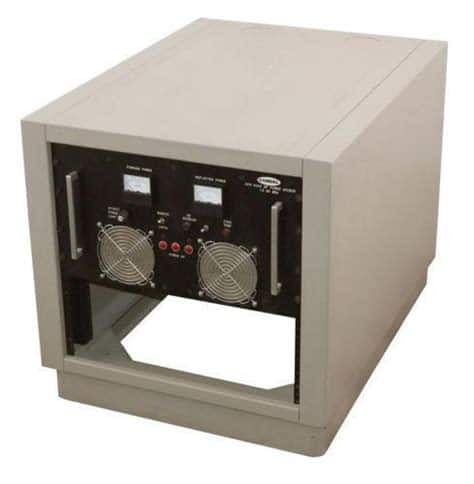
An RF power supply is a specialized electronic device that converts electrical energy into high-frequency alternating current (AC) suitable for driving RF loads, such as antennas, amplifiers, and transmitters. These power supplies typically operate at frequencies ranging from a few megahertz (MHz) to several gigahertz (GHz), depending on the specific application.
Key Components of an RF Power Supply
An RF power supply consists of several essential components that work together to generate and regulate the desired output:
-
Power Source: The primary power source can be AC mains, batteries, or a combination of both, depending on the application and power requirements.
-
Rectifier: The rectifier converts the AC input into pulsating DC, which is then smoothed by the filter capacitors.
-
Filter: The filter section, comprising capacitors and inductors, removes the ripple from the rectified DC and provides a clean, stable DC voltage to the subsequent stages.
-
DC-to-RF Converter: This stage, often implemented using a high-frequency switching topology, converts the DC voltage into the desired RF output. Common topologies include Class-E, Class-D, and Class-F amplifiers.
-
Matching Network: The matching network ensures proper impedance matching between the RF power supply and the load, maximizing power transfer and minimizing reflections.
-
Control and Protection Circuitry: Additional circuitry is incorporated to monitor and control the output power, frequency, and other parameters, as well as to protect the power supply and load from overload, overvoltage, and other fault conditions.
Designing an RF Power Supply
Step 1: Determine Power Requirements
The first step in designing an RF power supply is to determine the power requirements of the target application. This includes specifying the output power, frequency range, and load impedance. These parameters will guide the selection of components and the overall design approach.
Step 2: Select the Appropriate Topology
Based on the power requirements and frequency range, choose a suitable RF power supply topology. Common topologies include:
- Class-E: Highly efficient, single-ended topology suitable for high-frequency applications
- Class-D: Push-pull topology with high efficiency and wide frequency range
- Class-F: Harmonic-tuned topology that achieves high efficiency by shaping the output waveform
Consider factors such as efficiency, linearity, and complexity when selecting the topology.
Step 3: Design the DC Power Stage
The DC power stage consists of the rectifier, filter, and any necessary voltage regulation. Design this stage to provide a clean, stable DC voltage to the RF converter. Consider the following:
- Rectifier topology (half-wave, full-wave, or bridge)
- Filter capacitor selection (value, voltage rating, and ESR)
- Voltage regulation (linear or switching regulators)
Step 4: Design the RF Converter
Design the RF converter stage based on the selected topology. This involves choosing the appropriate transistors, inductors, capacitors, and other components to achieve the desired output power and frequency. Use simulation tools to optimize the design for efficiency and performance.
Step 5: Implement the Matching Network
Design the matching network to ensure proper impedance matching between the RF power supply and the load. This typically involves a combination of inductors and capacitors arranged in an L, Pi, or T network configuration. Use simulation tools and network analyzers to fine-tune the matching network for optimal performance.
Step 6: Incorporate Control and Protection Circuitry
Add control and protection circuitry to monitor and regulate the output power, frequency, and other parameters. This may include:
- Power control loops (e.g., ALC, AGC)
- Frequency synthesizers or VCOs for frequency control
- Overload, overvoltage, and thermal protection circuits
Ensure that the control and protection circuitry is properly integrated with the main RF power supply design.

PCB Layout Considerations
Proper PCB layout is crucial for the optimal performance and reliability of an RF power supply. Follow these guidelines when designing the PCB:
-
Ground Plane: Use a solid, uninterrupted ground plane to provide a low-impedance return path for high-frequency currents. Avoid splitting the ground plane, as this can create unwanted resonances and affect signal integrity.
-
Power Plane: Dedicate a separate power plane for the DC supply to minimize noise coupling and ensure a stable voltage distribution. Use appropriate decoupling capacitors near the power pins of active components.
-
Component Placement: Place components strategically to minimize trace lengths and reduce parasitics. Keep high-frequency components close to each other and to their respective ground and power connections.
-
Trace Routing: Route high-frequency traces as short and direct as possible, avoiding sharp bends and maintaining consistent trace width. Use microstrip or stripline techniques for controlled impedance traces.
-
Shielding: Implement proper shielding techniques to minimize electromagnetic interference (EMI) and crosstalk between different sections of the RF power supply. Use ground shields, compartmentalization, and RF-tight enclosures as needed.
-
Thermal Management: Consider the thermal requirements of the RF power supply and incorporate appropriate heat sinking and cooling mechanisms. Use thermal vias and heat spreaders to dissipate heat from power components.

Testing and Troubleshooting
Once the RF power supply is designed and fabricated, thorough testing and troubleshooting are essential to ensure its proper functioning and reliability. Follow these steps:
-
Visual Inspection: Perform a visual inspection of the assembled PCB to identify any manufacturing defects, such as incorrect component placement, solder bridges, or damaged traces.
-
Power-Up Tests: Gradually apply power to the RF power supply and monitor the DC voltages at various test points. Verify that the voltages are within the expected ranges and that there are no signs of overheating or abnormal behavior.
-
Frequency and Power Measurements: Use a spectrum analyzer or power meter to measure the output frequency and power of the RF power supply. Ensure that the measured values match the design specifications.
-
Load Tests: Connect the RF power supply to the intended load (or an equivalent dummy load) and monitor its performance under various operating conditions. Check for any signs of instability, excessive heating, or degraded performance.
-
EMI and Compliance Tests: Conduct electromagnetic compatibility (EMC) tests to ensure that the RF power supply meets the relevant EMI and regulatory requirements for its intended application and operating environment.
If any issues are encountered during testing, use systematic troubleshooting techniques to isolate the problem. Common troubleshooting steps include:
- Checking for proper power supply voltages and current limits
- Verifying component values and orientations
- Inspecting solder joints and trace integrity
- Probing signals with an oscilloscope to identify anomalies
- Comparing measured performance with simulation results
Frequently Asked Questions (FAQ)
1. What are the main differences between linear and switching RF power supplies?
Linear RF power supplies use linear voltage regulators to provide a stable DC voltage to the RF converter, while switching RF power supplies employ high-frequency switching techniques (e.g., PWM) to regulate the voltage. Switching power supplies are generally more efficient and compact, but they may introduce more noise and require additional filtering compared to linear power supplies.
2. How do I select the appropriate transistor for my RF power supply design?
When selecting a transistor for an RF power supply, consider factors such as the required output power, frequency range, gain, efficiency, and package type. Consult the transistor’s datasheet and application notes to ensure that it meets the design requirements and is suitable for the chosen topology. It’s also essential to consider the transistor’s thermal characteristics and the available cooling methods.
3. What are the main challenges in designing high-frequency RF power supplies?
High-frequency RF power supplies pose several design challenges, including:
- Minimizing parasitics and layout-induced impedance mismatches
- Ensuring proper heat dissipation and thermal management
- Achieving high efficiency while maintaining linearity and signal integrity
- Mitigating EMI and complying with regulatory standards
- Selecting components with suitable high-frequency characteristics
Careful design, simulation, and iterative optimization are necessary to overcome these challenges and achieve the desired performance.
4. How can I improve the efficiency of my RF power supply?
To improve the efficiency of an RF power supply, consider the following techniques:
- Choose a topology that inherently offers high efficiency, such as Class-E or Class-F
- Optimize the transistor biasing and drive levels for maximum efficiency
- Minimize losses in the matching network and passive components
- Use low-loss PCB materials and optimize the layout to reduce parasitics
- Implement efficient power control and voltage regulation techniques
- Employ resonant switching techniques to minimize switching losses
Continuously monitor and optimize the efficiency throughout the design process, using simulation tools and practical measurements.
5. What are some common troubleshooting techniques for RF power supplies?
Common troubleshooting techniques for RF power supplies include:
- Checking for proper power supply voltages and current limits
- Verifying component values and orientations
- Inspecting solder joints and trace integrity
- Probing signals with an oscilloscope to identify anomalies
- Comparing measured performance with simulation results
- Isolating sections of the circuit to pinpoint the source of the issue
- Substituting components with known-good ones to rule out component failures
A systematic and methodical approach to troubleshooting, combined with a thorough understanding of the RF power supply’s design and expected behavior, is essential for effective problem resolution.
Conclusion
Designing and laying out an RF power supply requires a comprehensive understanding of RF principles, power electronics, and PCB design techniques. By following the guidelines and best practices outlined in this article, engineers can develop efficient, reliable, and high-performance RF power supplies for a wide range of applications.
Proper component selection, circuit topology choice, and PCB layout are critical factors in achieving the desired output power, frequency, and efficiency. Additionally, thorough testing and troubleshooting are essential to ensure the RF power supply meets the specified requirements and operates reliably in its intended environment.
As RF technology continues to evolve and find new applications, the demand for well-designed RF power supplies will continue to grow. By staying up-to-date with the latest design techniques and tools, RF engineers can tackle the challenges associated with high-frequency power supply design and contribute to the advancement of wireless technologies.
No responses yet