Introduction to RF-PCB-Layout
Designing a printed circuit board (PCB) for radio frequency (RF) applications requires careful consideration of various factors to ensure optimal performance. One critical aspect of RF-PCB-Layout is the implementation of RF filters, which are essential components in many wireless systems. This article provides an in-depth exploration of RF filter PCB layout techniques, guidelines, and best practices to help engineers and designers achieve successful designs.
Understanding RF Filters
Types of RF Filters
RF filters are electronic circuits designed to selectively pass or attenuate specific frequency ranges while rejecting others. There are several types of RF filters commonly used in PCB designs:
- Low-pass filters (LPF): Allow frequencies below a specified cutoff frequency to pass while attenuating higher frequencies.
- High-pass filters (HPF): Allow frequencies above a specified cutoff frequency to pass while attenuating lower frequencies.
- Band-pass filters (BPF): Allow a specific range of frequencies to pass while attenuating frequencies outside that range.
- Band-stop filters (BSF) or notch filters: Attenuate a specific range of frequencies while allowing frequencies outside that range to pass.
Filter Topologies
RF filters can be implemented using various topologies, each with its own characteristics and design considerations. Some common filter topologies include:
- Lumped element filters: Consist of discrete components such as capacitors and inductors.
- Microstrip filters: Utilize microstrip transmission lines and open or short-circuited stubs.
- Coupled-line filters: Employ coupled microstrip or stripline transmission lines.
- Cavity filters: Use resonant cavities to achieve high-quality factors and sharp frequency selectivity.
RF-PCB-Layout Considerations
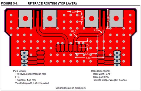
Substrate Selection
The choice of substrate material is crucial in RF-PCB-Layout. The substrate’s dielectric constant (εr) and loss tangent (tanδ) significantly impact the filter’s performance. Common substrate materials for RF applications include:
| Substrate Material | Dielectric Constant (εr) | Loss Tangent (tanδ) |
|---|---|---|
| FR-4 | 4.4 | 0.02 |
| Rogers RO4003C | 3.38 | 0.0027 |
| Rogers RT/duroid 5880 | 2.2 | 0.0009 |
Select a substrate with a stable dielectric constant and low loss tangent to minimize signal attenuation and ensure consistent filter performance.
Transmission Line Dimensions
Properly designing transmission lines is essential for RF filters. The width and spacing of microstrip or stripline traces determine the characteristic impedance and affect filter performance. Use impedance calculators or simulation tools to determine the appropriate trace dimensions based on the substrate properties and desired impedance.
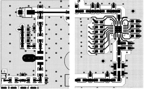
Component Placement and Routing
When placing components and routing traces for RF filters, consider the following guidelines:
- Minimize trace lengths to reduce parasitic inductance and capacitance.
- Avoid sharp bends or discontinuities in traces to minimize reflections and signal distortion.
- Maintain symmetry in component placement and routing to ensure balanced filter response.
- Provide adequate ground connections and ground planes to minimize ground inductance and ensure proper grounding.
Shielding and Isolation
RF filters require proper shielding and isolation to prevent electromagnetic interference (EMI) and crosstalk. Techniques for effective shielding and isolation include:
- Using ground planes and via fences to isolate filter sections from other circuit components.
- Implementing shielding enclosures or compartments to contain electromagnetic fields.
- Employing guard traces or ground rings around sensitive filter components to reduce coupling.

Filter Design and Simulation
Filter Design Tools
Several software tools are available for designing and simulating RF filters:
- Keysight ADS (Advanced Design System)
- Ansys HFSS (High-Frequency Structure Simulator)
- CST Studio Suite
- Agilent Genesys
These tools allow engineers to model and optimize filter designs, perform electromagnetic simulations, and analyze filter performance before physical implementation.
Simulation and Optimization
Simulate the RF filter design to evaluate its frequency response, insertion loss, return loss, and other key parameters. Optimize the design by adjusting component values, transmission line dimensions, and layout to achieve the desired filter characteristics.
Manufacturing and Testing
PCB Fabrication
When manufacturing RF filter PCBs, consider the following factors:
- Choose a reputable PCB fabrication vendor with experience in RF and high-frequency designs.
- Specify the required PCB material, layer stackup, and copper thickness to ensure consistent performance.
- Communicate any special requirements, such as controlled impedance or tight tolerances, to the fabrication vendor.
Testing and Validation
After fabricating the RF filter PCB, perform thorough testing and validation to ensure its performance meets the design specifications:
- Use a vector network analyzer (VNA) to measure the filter’s frequency response, insertion loss, and return loss.
- Verify the filter’s isolation and rejection of unwanted frequencies.
- Conduct EMI and electromagnetic compatibility (EMC) tests to ensure the filter meets regulatory requirements.
Best Practices and Guidelines
- Keep RF filter sections as compact as possible to minimize parasitic effects.
- Use a solid ground plane underneath the filter to provide a low-impedance return path.
- Avoid routing other signals or traces near the filter to prevent coupling and interference.
- Use via stitching or fencing around the filter to create a Faraday cage and improve shielding.
- Implement impedance matching techniques, such as tapered lines or matching networks, to optimize filter performance.
- Consider the effect of component tolerances and variations on filter performance during the design phase.
- Follow the manufacturer’s guidelines for component placement, soldering, and handling.
- Perform post-layout simulations to verify the filter’s performance considering PCB parasitics.
Frequently Asked Questions (FAQ)
-
Q: What is the purpose of an RF filter in a PCB design?
A: RF filters are used to selectively pass or attenuate specific frequency ranges while rejecting others, helping to remove unwanted signals, reduce interference, and improve the overall performance of the RF system. -
Q: How do I choose the right substrate material for my RF filter PCB?
A: When selecting a substrate material, consider factors such as the dielectric constant, loss tangent, and frequency range of operation. Materials with a stable dielectric constant and low loss tangent, such as Rogers RO4003C or RT/duroid 5880, are commonly used for RF applications. -
Q: What are the consequences of improper grounding in an RF filter PCB layout?
A: Improper grounding can lead to ground loops, increased ground inductance, and poor filter performance. It can result in signal integrity issues, increased noise, and degraded frequency response. -
Q: How can I minimize coupling and interference between the RF filter and other circuit components?
A: To minimize coupling and interference, use shielding techniques such as ground planes, via fences, and shielding enclosures. Maintain adequate spacing between the filter and other components, and avoid routing other signals or traces near the filter. -
Q: What are the key parameters to consider when testing and validating an RF filter PCB?
A: When testing and validating an RF filter PCB, important parameters to consider include the frequency response, insertion loss, return loss, isolation, and rejection of unwanted frequencies. Use a vector network analyzer (VNA) to measure these parameters and ensure they meet the design specifications.
Conclusion
Designing an RF filter PCB layout requires careful consideration of various factors, including substrate selection, transmission line dimensions, component placement, routing, shielding, and simulation. By following best practices and guidelines, engineers can optimize the filter’s performance, minimize interference, and ensure reliable operation in RF systems.
Effective RF-PCB-Layout techniques, combined with thorough simulation, manufacturing, and testing processes, enable the successful implementation of RF filters in a wide range of applications, from wireless communications to radar systems and beyond.
No responses yet