What is PCB Reverse Engineering?
PCB reverse engineering is the process of analyzing a printed circuit board (PCB) to understand its design, functionality, and components. It involves examining the physical board, identifying components, tracing connections, and creating a schematic or design file based on the gathered information. The goal is to recreate the original design documentation or to understand how the board functions.
Why Perform PCB Reverse Engineering?
There are several reasons why someone might need to reverse engineer a PCB:
-
Obsolescence: When the original manufacturer no longer produces a particular PCB, reverse engineering can help create a replacement or compatible board.
-
Lack of documentation: If the original design files or schematics are lost or unavailable, reverse engineering can help recreate the necessary documentation.
-
Modification or improvement: Understanding the design of an existing PCB can enable modifications or improvements to be made to the board’s functionality.
-
Competitive analysis: Reverse engineering can be used to understand the design and functionality of a competitor’s product.
Applications of PCB Reverse Engineering
PCB reverse engineering finds applications in various fields, including:
-
Electronics manufacturing: Recreating obsolete or hard-to-find PCBs for replacement or repair purposes.
-
Military and aerospace: Analyzing and reproducing PCBs used in critical systems for maintenance and upgrades.
-
Automotive industry: Understanding and reproducing PCBs used in vehicles for repair and customization.
-
Consumer electronics: Analyzing competitor products or creating compatible accessories.
The PCB Reverse Engineering Process
The process of reverse engineering a PCB typically involves the following steps:
1. Visual Inspection
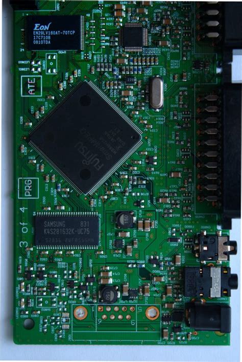
The first step is to visually examine the PCB to identify components, connectors, and any visible markings or labels. This helps in understanding the overall layout and functionality of the board.
2. Component Identification
Each component on the PCB needs to be identified and documented. This includes identifying the component type (resistor, capacitor, IC, etc.), value (resistance, capacitance, IC part number), and package (SMD, through-hole). Datasheets for the identified components can provide valuable information about their functionality and pinout.
| Component Type | Identification Method |
|---|---|
| Resistors | Color code, value printed on the component |
| Capacitors | Value printed on the component, physical size |
| ICs | Part number printed on the component, package type |
| Diodes | Part number, polarity marking |
| Transistors | Part number, package type, pinout |
3. Tracing Connections
The next step is to trace the connections between components. This can be done manually using a multimeter or continuity tester or with the help of specialized tools like a PCB scanner or X-ray machine. The goal is to determine how the components are interconnected and to identify any power and ground connections.
4. Creating a Schematic
Based on the information gathered from component identification and connection tracing, a schematic of the PCB can be created. This schematic represents the logical connections between components and helps in understanding the circuit’s functionality. Schematic capture software like KiCad, Eagle, or Altium Designer can be used for this purpose.
5. Creating a PCB Layout
Once the schematic is complete, a PCB layout can be created. This involves placing the components on a virtual board and routing the connections between them. The layout should closely match the physical board being reverse engineered. PCB design software is used for this step.
6. Verification and Testing
After creating the schematic and PCB layout, it’s important to verify the design by comparing it with the original board. This can involve visual inspection, continuity testing, and functional testing. Any discrepancies should be identified and corrected.

Tools for PCB Reverse Engineering
Several tools can assist in the PCB reverse engineering process:
-
Multimeter or continuity tester: Used for manually tracing connections and verifying continuity.
-
PCB scanner: Automated tool that scans the PCB and creates a digital image of the board, helping in component identification and connection tracing.
-
X-ray machine: Allows non-destructive imaging of the internal layers and connections of a multi-layer PCB.
-
Microscope: Helps in visual inspection and identification of small components and markings.
-
Schematic capture and PCB design software: Tools like KiCad, Eagle, or Altium Designer are used for creating schematics and PCB layouts based on the reverse engineered data.

Challenges in PCB Reverse Engineering
PCB reverse engineering can be a complex and time-consuming process. Some of the challenges include:
-
Component identification: Identifying components, especially unmarked or custom components, can be difficult.
-
Multi-layer boards: Reverse engineering multi-layer PCBs requires specialized tools like X-ray machines to trace connections between layers.
-
Incomplete or damaged boards: If the original PCB is damaged or has missing components, it can be challenging to recreate the complete design.
-
Legal considerations: Reverse engineering may be subject to legal restrictions, especially if the PCB design is protected by intellectual property rights.

Frequently Asked Questions (FAQ)
-
Is PCB reverse engineering legal?
The legality of PCB reverse engineering depends on the specific circumstances and jurisdiction. In general, reverse engineering for the purpose of interoperability, repair, or analysis is legal in many countries. However, if the reverse engineering process violates intellectual property rights or is used for unlawful purposes, it may be considered illegal. It’s important to consult with legal experts to understand the specific laws and regulations applicable to your situation. -
How accurate is PCB reverse engineering?
The accuracy of PCB reverse engineering depends on various factors, including the complexity of the board, the tools used, and the skill of the person performing the reverse engineering. With proper techniques and tools, a high level of accuracy can be achieved. However, it’s important to verify the recreated design against the original board to ensure correctness. -
Can PCB reverse engineering be used for product cloning?
While PCB reverse engineering can be used to understand and recreate the design of a product, using it for unauthorized cloning or counterfeiting is generally illegal. Reverse engineering should be used responsibly and ethically, respecting intellectual property rights and legal boundaries. -
How long does PCB reverse engineering take?
The time required for PCB reverse engineering varies depending on the complexity of the board, the tools available, and the experience of the person performing the reverse engineering. Simple boards may take a few hours to a few days, while complex multi-layer boards can take several weeks or even months. The process can be time-consuming and requires patience and attention to detail. -
Are there any automated tools for PCB reverse engineering?
There are several automated tools that can assist in PCB reverse engineering, such as PCB scanners and X-ray machines. These tools can help in component identification, connection tracing, and creating digital representations of the board. However, automated tools have limitations and may not be able to capture all the details, especially for complex or custom designs. Manual interpretation and analysis are still crucial in the reverse engineering process.
Conclusion
PCB reverse engineering is a valuable technique for understanding and recreating the design of a printed circuit board when the original documentation is unavailable or the board needs to be modified or reproduced. It involves a systematic process of visual inspection, component identification, connection tracing, schematic creation, and PCB layout design.
While PCB reverse engineering can be challenging and time-consuming, it finds applications in various fields, including electronics manufacturing, military and aerospace, automotive, and consumer electronics. With the help of appropriate tools and techniques, accurate and detailed reverse engineering of PCBs is possible.
However, it’s important to approach PCB reverse engineering responsibly and ethically, respecting intellectual property rights and legal boundaries. Consulting with legal experts and following applicable laws and regulations is crucial when engaging in reverse engineering activities.
By understanding the process, tools, and challenges involved in PCB reverse engineering, engineers and technicians can effectively recreate and analyze PCB designs, enabling repair, modification, and reproduction of electronic systems.
No responses yet