Introduction to Dielectric Permittivity
Dielectric permittivity, also known as relative permittivity or εr, is a crucial property of insulating materials used in printed circuit boards (PCBs). It measures the ability of a material to store electrical energy in an electric field. The dielectric permittivity of a material is expressed as a ratio relative to the permittivity of free space (ε0), which has a value of approximately 8.85 × 10^-12 F/m.
Factors Influencing Dielectric Permittivity
Several factors can influence the dielectric permittivity of a material:
- Material composition
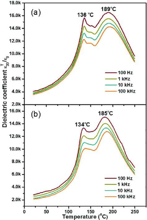
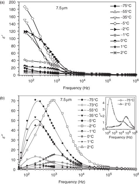
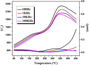
- Frequency of the applied electric field
- Temperature
- Humidity
- Impurities or additives
PCB Substrates and Dielectric Permittivity
PCB substrates are the insulating materials upon which conductive traces and components are placed. The choice of substrate material is essential for the performance, reliability, and cost of the PCB. One of the key properties to consider when selecting a PCB substrate is its dielectric permittivity.
Common PCB Substrate Materials and Their Dielectric Permittivity
| Material | Dielectric Permittivity (εr) |
|---|---|
| FR-4 (Glass-reinforced Epoxy) | 4.2 – 4.9 |
| Rogers RO4003C | 3.38 |
| Rogers RT/duroid 5880 | 2.20 |
| Polyimide | 3.4 – 3.5 |
| PTFE (Polytetrafluoroethylene) | 2.1 |
| Alumina (Ceramic) | 9.8 |
Impact of Dielectric Permittivity on PCB Performance
The dielectric permittivity of a PCB substrate can have a significant impact on the performance of the circuit, particularly at high frequencies. Some of the effects include:
- Signal propagation speed: Lower permittivity materials allow signals to travel faster, which is crucial for high-speed applications.
- Characteristic impedance: The characteristic impedance of a transmission line is influenced by the dielectric permittivity of the substrate. Matching the impedance is essential for minimizing signal reflections and ensuring proper signal integrity.
- Crosstalk: Higher permittivity materials can increase the capacitive coupling between adjacent traces, leading to increased crosstalk.
- Power dissipation: Materials with higher dielectric permittivity often have higher dielectric loss tangents, which can result in increased power dissipation and heating.
High-K and Low-K Dielectrics
Dielectric materials can be classified as high-K or low-K based on their relative permittivity values.
High-K Dielectrics
High-K dielectrics are materials with a relative permittivity significantly higher than that of silicon dioxide (εr ≈ 3.9). These materials are often used in applications where high capacitance is required, such as in decoupling capacitors or gate dielectrics in transistors. Some examples of high-K dielectrics include:
- Hafnium dioxide (HfO2): εr ≈ 25
- Zirconium dioxide (ZrO2): εr ≈ 25
- Barium strontium titanate (BST): εr > 200
- Tantalum pentoxide (Ta2O5): εr ≈ 22
Advantages of High-K Dielectrics
- Increased capacitance density
- Reduced leakage current
- Potential for miniaturization
Disadvantages of High-K Dielectrics
- Higher dielectric loss tangent
- Increased manufacturing complexity
- Potential for thermal instability
Low-K Dielectrics
Low-K dielectrics are materials with a relative permittivity lower than that of silicon dioxide. These materials are valuable for reducing parasitic capacitance, signal delay, and power consumption in high-speed digital circuits. Some examples of low-K dielectrics include:
- Polyimide: εr ≈ 3.4 – 3.5
- Benzocyclobutene (BCB): εr ≈ 2.6 – 2.7
- SiLK (Semiconductor dielectric resin): εr ≈ 2.7
- Porous silicon dioxide: εr < 3.0
Advantages of Low-K Dielectrics
- Reduced signal propagation delay
- Lower power consumption
- Decreased crosstalk
- Improved signal integrity
Disadvantages of Low-K Dielectrics
- Reduced mechanical strength
- Increased moisture absorption
- Potential for thermal expansion mismatch
- Higher manufacturing costs

Choosing the Right Dielectric for PCB Substrates
When selecting a PCB substrate material, several factors should be considered in addition to the dielectric permittivity:
- Frequency of operation
- Thermal requirements
- Mechanical requirements
- Cost
- Manufacturability
For high-speed digital applications, low-K dielectrics are generally preferred, as they minimize signal propagation delay and reduce power consumption. However, if mechanical strength or thermal stability is a concern, a substrate with a higher dielectric permittivity may be more suitable.
In RF and microwave applications, the choice of substrate material is critical for achieving the desired performance. Low-loss materials with a consistent dielectric permittivity over the frequency range of interest are essential. PTFE-based substrates, such as Rogers RT/duroid 5880, are popular choices for these applications.
Future Trends in PCB Substrate Materials
As electronic devices continue to push the boundaries of performance and miniaturization, new substrate materials with improved dielectric properties are being developed. Some of the emerging trends in PCB substrate materials include:
- Ultra-low-K dielectrics: Materials with a relative permittivity below 2.0 are being explored to further reduce parasitic capacitance and signal delay.
- High-temperature materials: Substrates that can withstand extreme temperatures (>200°C) are in demand for automotive, aerospace, and industrial applications.
- Flexible and stretchable substrates: The growth of wearable electronics and the Internet of Things (IoT) has driven the development of flexible and stretchable substrate materials that can conform to various shapes and surfaces.
- Environmentally friendly materials: There is an increasing focus on developing substrate materials that are recyclable, biodegradable, and free from hazardous substances.
Frequently Asked Questions (FAQ)
-
What is the difference between high-K and low-K dielectrics?
High-K dielectrics have a relative permittivity significantly higher than that of silicon dioxide (εr ≈ 3.9), while low-K dielectrics have a relative permittivity lower than that of silicon dioxide. High-K dielectrics are used for applications requiring high capacitance, while low-K dielectrics are used for reducing parasitic capacitance and signal delay. -
Why is the dielectric permittivity important for PCB substrates?
The dielectric permittivity of a PCB substrate influences signal propagation speed, characteristic impedance, crosstalk, and power dissipation. Choosing the right dielectric permittivity is crucial for ensuring proper circuit performance, particularly at high frequencies. -
What is the most common PCB substrate material?
FR-4, a glass-reinforced epoxy laminate, is the most widely used PCB substrate material. It offers a good balance of mechanical, thermal, and electrical properties at a relatively low cost. -
What are the advantages of using low-K dielectrics in high-speed digital circuits?
Low-K dielectrics reduce signal propagation delay, lower power consumption, decrease crosstalk, and improve signal integrity in high-speed digital circuits. These advantages are crucial for maintaining proper circuit performance as operating frequencies continue to increase. -
What factors should be considered when selecting a PCB substrate material?
When choosing a PCB substrate material, consider the frequency of operation, thermal requirements, mechanical requirements, cost, and manufacturability, in addition to the dielectric permittivity. The optimal substrate material will depend on the specific application and design requirements.
Conclusion
Understanding the role of dielectric permittivity in PCB substrates is essential for designing high-performance electronic circuits. The choice between high-K and low-K dielectrics depends on the specific application requirements, such as the need for high capacitance or low signal propagation delay.
As technology advances, new substrate materials with improved dielectric properties will continue to be developed to meet the ever-increasing demands for performance, reliability, and sustainability. By staying informed about the latest trends and materials in PCB substrate technology, designers can make informed decisions and create innovative electronic products that push the boundaries of what is possible.
No responses yet