Introduction to PCB Ground Recovery
Printed Circuit Boards (PCBs) are essential components in modern electronics, providing a platform for interconnecting various electronic components. One of the critical aspects of PCB design is the proper management of the ground layer. The ground layer plays a vital role in ensuring signal integrity, reducing electromagnetic interference (EMI), and maintaining stable reference voltages. However, due to various factors such as manufacturing defects, improper design, or environmental conditions, the ground layer can suffer from conductor losses, leading to degraded performance and reliability issues. In this article, we will explore the concept of PCB ground recovery, its importance, and the techniques used to restore the integrity of the ground layer.
Understanding Conductor Losses in PCBs
Conductor losses in PCBs refer to the unwanted dissipation of electrical energy as heat due to the resistance of the conductive traces. These losses can occur in both the signal traces and the ground layer. When it comes to the ground layer, conductor losses can have a significant impact on the overall performance of the PCB. Some of the factors that contribute to conductor losses in the ground layer include:
-
Thin copper thickness: If the copper thickness of the ground layer is insufficient, it can lead to increased resistance and higher losses.
-
Improper ground plane design: Poor ground plane design, such as inadequate copper coverage or discontinuities in the ground plane, can disrupt the flow of return currents and introduce losses.
-
High-frequency signals: As the frequency of the signals increases, the skin effect becomes more prominent, causing current to flow primarily on the surface of the conductor. This can lead to increased losses in the ground layer.
-
Manufacturing defects: Defects introduced during the manufacturing process, such as uneven copper distribution or voids in the ground plane, can contribute to conductor losses.
Importance of PCB Ground Recovery
Recovering conductor losses in the ground layer is crucial for several reasons:
-
Signal integrity: A well-designed and intact ground layer provides a low-impedance return path for signals, minimizing signal distortion and ensuring proper signal propagation.
-
EMI reduction: A continuous and uninterrupted ground plane helps in reducing electromagnetic interference by providing a shield against unwanted radiation.
-
Power distribution: The ground layer acts as a reference plane for power distribution, helping to maintain stable voltage levels and reducing voltage drops across the PCB.
-
Thermal management: Efficient heat dissipation is essential for the reliable operation of electronic components. A well-designed ground layer helps in spreading heat evenly across the PCB, preventing hot spots and thermal stress.

Techniques for PCB Ground Recovery
Several techniques can be employed to recover conductor losses in the ground layer and restore its integrity:
1. Copper Thieving
Copper thieving is a technique used to improve the uniformity of copper distribution in the ground layer. It involves adding small copper shapes or patterns in areas where there is excess copper, such as around the edges of the PCB or in regions with sparse component placement. By redistributing the copper, copper thieving helps in reducing conductor losses and improving the overall ground plane continuity.
2. Ground Plane Stitching
Ground plane stitching is a method used to establish a low-impedance connection between different ground planes or regions on the PCB. It involves placing vias or conductive traces to connect the ground planes, ensuring a continuous and uninterrupted ground reference. Ground plane stitching is particularly important in multi-layer PCBs, where different ground planes may exist on different layers.
3. Via Shielding
Via shielding is a technique used to reduce the coupling of high-frequency signals into the ground layer through vias. It involves surrounding the signal vias with ground vias, creating a shielding effect and minimizing the interference caused by the signal vias. Via shielding helps in maintaining the integrity of the ground layer and reducing conductor losses.
4. Optimizing Copper Thickness
Increasing the copper thickness of the ground layer can help in reducing conductor losses. Thicker copper provides lower resistance and better heat dissipation capabilities. However, it is essential to strike a balance between copper thickness and manufacturing feasibility. Designers should consider the manufacturing capabilities and cost implications when deciding on the copper thickness for the ground layer.
5. Proper Ground Plane Design
Proper ground plane design is crucial for minimizing conductor losses and ensuring optimal performance. Some key considerations include:
- Maintaining a continuous and uninterrupted ground plane throughout the PCB.
- Avoiding unnecessary slots or cuts in the ground plane, as they can disrupt the flow of return currents.
- Providing adequate copper coverage and avoiding large void areas in the ground plane.
- Placing ground vias strategically to establish a low-impedance connection between components and the ground plane.

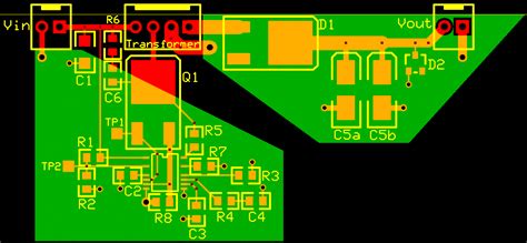
Case Study: Recovering Conductor Losses in a High-Speed Digital PCB
To illustrate the application of PCB ground recovery techniques, let’s consider a case study of a high-speed digital PCB design.
Problem Statement
A high-speed digital PCB was experiencing signal integrity issues and intermittent failures during operation. The PCB contained multiple high-frequency digital signals, and the ground layer was suspected to be the root cause of the problem.
Analysis and Findings
Upon analyzing the PCB layout and conducting measurements, the following issues were identified:
- Insufficient copper thickness in the ground layer, leading to increased resistance and conductor losses.
- Discontinuities in the ground plane due to improper placement of components and routing of signal traces.
- Lack of proper via shielding for high-frequency signals, resulting in coupling and interference.
Solution and Implementation
To recover the conductor losses and improve the ground layer integrity, the following steps were taken:
- The copper thickness of the ground layer was increased from 1 oz to 2 oz to reduce resistance and improve heat dissipation.
- Copper thieving techniques were applied in regions with excess copper to achieve a more uniform distribution.
- Ground plane stitching was implemented to establish a continuous ground reference between different layers of the PCB.
- Via shielding was added for high-frequency signals to minimize coupling and interference.
- The placement of components and routing of signal traces were optimized to avoid discontinuities in the ground plane.
Results and Benefits
After implementing the PCB ground recovery techniques, the following results were observed:
- Signal integrity improved significantly, with reduced signal distortion and cleaner waveforms.
- The intermittent failures during operation were eliminated, resulting in improved reliability.
- EMI levels were reduced, meeting the required regulatory standards.
- The overall thermal performance of the PCB improved, with better heat dissipation and reduced hot spots.
The successful recovery of conductor losses in the ground layer through the application of appropriate techniques demonstrated the importance of proper ground plane design and the effectiveness of PCB ground recovery methods.
Frequently Asked Questions (FAQ)
-
What are conductor losses in PCBs?
Conductor losses in PCBs refer to the unwanted dissipation of electrical energy as heat due to the resistance of the conductive traces, including the ground layer. -
Why is it important to recover conductor losses in the ground layer?
Recovering conductor losses in the ground layer is important for maintaining signal integrity, reducing EMI, ensuring proper power distribution, and achieving effective thermal management. -
What are some techniques used for PCB ground recovery?
Some common techniques used for PCB ground recovery include copper thieving, ground plane stitching, via shielding, optimizing copper thickness, and proper ground plane design. -
How does copper thickness affect conductor losses in the ground layer?
Increasing the copper thickness of the ground layer helps in reducing conductor losses by providing lower resistance and better heat dissipation capabilities. However, designers should consider manufacturing feasibility and cost implications when deciding on the copper thickness. -
What are the benefits of proper ground plane design in PCBs?
Proper ground plane design offers several benefits, including improved signal integrity, reduced EMI, stable power distribution, and effective thermal management. It ensures a continuous and uninterrupted ground reference throughout the PCB, minimizing conductor losses and enhancing overall performance and reliability.
Conclusion
PCB ground recovery is a crucial aspect of ensuring the proper functioning and reliability of electronic devices. Conductor losses in the ground layer can lead to signal integrity issues, EMI problems, and thermal management challenges. By understanding the factors contributing to conductor losses and applying appropriate techniques such as copper thieving, ground plane stitching, via shielding, and optimizing copper thickness, designers can effectively recover conductor losses and restore the integrity of the ground layer.
Proper ground plane design plays a vital role in minimizing conductor losses and achieving optimal performance. Maintaining a continuous and uninterrupted ground plane, avoiding unnecessary discontinuities, providing adequate copper coverage, and strategic placement of ground vias are key considerations in ground plane design.
The case study presented in this article demonstrates the practical application of PCB ground recovery techniques in a high-speed digital PCB. By addressing issues such as insufficient copper thickness, ground plane discontinuities, and lack of via shielding, the signal integrity and reliability of the PCB were significantly improved.
As technology advances and electronic devices become more complex, the importance of PCB ground recovery will continue to grow. Designers must stay updated with the latest techniques and best practices to ensure the integrity of the ground layer and deliver high-quality, reliable PCBs.
By understanding the concepts of conductor losses, implementing effective ground recovery techniques, and following proper ground plane design principles, designers can overcome the challenges associated with PCB ground recovery and create robust and reliable electronic products.
No responses yet