The Importance of PCB Design
The first and arguably most critical step in PCB Manufacturing is the design phase. A well-designed PCB lays the foundation for a successful manufacturing process and a reliable end product. Here are some essential aspects to consider when designing a PCB:
Schematic Design
- Create a clear and accurate schematic that represents the electrical connections and components of the circuit.
- Use standardized symbols and nomenclature for easy interpretation and communication with the manufacturing team.
- Perform thorough error checking and verification to catch any design flaws early on.
Component Selection
- Choose components that are readily available, reliable, and suitable for the intended application.
- Consider factors such as package size, power rating, and temperature tolerance when selecting components.
- Ensure compatibility between components and the PCB substrate material.
Layout Design
- Follow best practices for PCB layout, including proper trace width, spacing, and routing.
- Minimize the length of high-speed signal traces to reduce signal integrity issues.
- Incorporate appropriate ground planes and power distribution networks to ensure stable power delivery and reduce noise.
- Consider the mechanical dimensions and constraints of the PCB, including mounting holes and connector placements.
Design for Manufacturability (DFM)
- Adhere to the manufacturing capabilities and limitations of the chosen PCB fabrication process.
- Maintain appropriate clearances and tolerances for copper traces, solder mask, and silkscreen.
- Avoid unnecessarily small or tight features that may pose challenges during fabrication.
- Communicate any special requirements or constraints to the manufacturing team upfront.
Material Selection
The choice of materials used in PCB manufacturing has a significant impact on the performance, reliability, and cost of the final product. Here are some key considerations for material selection:
PCB Substrate Material
- FR-4 is the most common and cost-effective substrate material for general-purpose PCBs.
- High-frequency or high-speed applications may require specialized materials like Rogers or Isola.
- Consider the dielectric constant, loss tangent, and thermal properties of the substrate material.
Copper Thickness
- Choose the appropriate copper thickness based on the current carrying requirements and trace width.
- Thicker copper layers provide better current handling capacity but may increase the cost and weight of the PCB.
Solder Mask and Silkscreen
- Select a solder mask color (green, red, blue, etc.) that provides good contrast and readability.
- Ensure the solder mask apertures are appropriately sized to prevent solder bridging or poor solder wetting.
- Use clear and concise silkscreen legends to aid in component placement and identification.
| Material | Typical Applications | Key Properties |
|---|---|---|
| FR-4 | General-purpose PCBs | Low cost, good mechanical and electrical properties |
| Rogers | High-frequency, RF, and microwave applications | Low dielectric loss, stable dielectric constant |
| Isola | High-speed digital and RF applications | Low loss, low dielectric constant, high thermal stability |
| Copper (1 oz.) | Low to medium current carrying traces | Good conductivity, cost-effective |
| Copper (2 oz.) | High current carrying traces, power planes | Excellent current handling capacity, higher cost |
Table: Common PCB Materials and Their Properties

PCB Fabrication Processes
Once the design is finalized and the materials are selected, the PCB undergoes various fabrication processes to transform it from a digital design to a physical board. Let’s take a closer look at the key fabrication steps:
Copper Etching
- The copper layer is selectively removed using a chemical etching process to create the desired trace patterns.
- Common etching methods include subtractive (e.g., photoresist and etch) and additive (e.g., pattern plating) processes.
- Proper control of the etching parameters ensures accurate trace widths and spacing.
Drilling
- Holes are drilled through the PCB substrate to accommodate through-hole components and vias.
- Mechanical drilling is the most common method, using high-speed drill bits.
- Laser drilling can be used for smaller, more precise holes.
Plating
- The drilled holes are plated with a conductive material (usually copper) to create electrical connections between layers.
- Electroless and electrolytic plating techniques are used to deposit the conductive material.
- Proper plating thickness and uniformity are crucial for reliable electrical connections.
Solder Mask Application
- A solder mask layer is applied to the PCB surface to protect the copper traces from oxidation and prevent solder bridging.
- Liquid photoimageable (LPI) solder masks are commonly used, which are applied as a liquid and then exposed and developed.
- The solder mask should have good adhesion, durability, and resistance to environmental factors.
Silkscreen Printing
- The silkscreen layer is printed on top of the solder mask to provide component labels, logos, and other markings.
- Screen printing is the most common method, using a fine mesh screen and ink.
- The silkscreen should be legible, durable, and resistant to abrasion and chemicals.
| Process | Purpose | Key Considerations |
|---|---|---|
| Copper Etching | Create desired trace patterns | Accurate trace widths and spacing |
| Drilling | Create holes for components and vias | Proper hole size and positioning |
| Plating | Establish electrical connections between layers | Uniform plating thickness and coverage |
| Solder Mask | Protect traces and prevent solder bridging | Good adhesion, durability, and environmental resistance |
| Silkscreen | Provide component labels and markings | Legibility, durability, and abrasion resistance |
Table: PCB Fabrication Processes and Key Considerations

Quality Control and Testing
To ensure the manufactured PCBs meet the required specifications and perform reliably, rigorous quality control and testing procedures are implemented throughout the manufacturing process. Here are some essential aspects of quality control and testing:
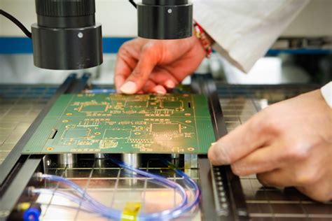
Visual Inspection
- Visually inspect the PCBs for any obvious defects, such as missing components, solder bridges, or damaged traces.
- Use magnification tools or automated optical inspection (AOI) systems for detailed examination.
Electrical Testing
- Perform continuity tests to verify the electrical connections between components and traces.
- Conduct isolation tests to ensure there are no short circuits or unintended connections.
- Perform functional tests to validate the PCB’s performance under various operating conditions.
Environmental Testing
- Subject the PCBs to environmental stress tests, such as temperature cycling, humidity exposure, and vibration testing.
- Evaluate the PCB’s ability to withstand the expected operating conditions and identify any potential weaknesses.
Automated Testing
- Utilize automated test equipment (ATE) to perform high-volume, repetitive testing.
- Develop test programs and fixtures to interface with the PCB and validate its functionality.
- Automated testing enables faster and more consistent testing compared to manual methods.
Statistical Process Control
- Implement statistical process control (SPC) techniques to monitor and control the manufacturing process.
- Collect and analyze data on key process parameters, such as etching times, plating thickness, and component placement accuracy.
- Use control charts and other statistical tools to detect process deviations and initiate corrective actions.

Documentation and Traceability
Proper documentation and traceability are essential for effective communication, quality control, and troubleshooting throughout the PCB manufacturing process. Here are some key points to consider:
Bill of Materials (BOM)
- Maintain an accurate and up-to-date bill of materials that lists all the components used in the PCB.
- Include component part numbers, quantities, and any special instructions or notes.
- Ensure the BOM is reviewed and approved by the relevant stakeholders.
Fabrication Drawings
- Create detailed fabrication drawings that specify the PCB dimensions, layer stackup, and manufacturing requirements.
- Include notes on any special processes, tolerances, or materials required.
- Use clear and standardized formatting to avoid ambiguity and misinterpretation.
Revision Control
- Implement a robust revision control system to track changes made to the PCB design and manufacturing process.
- Assign unique revision numbers or identifiers to each version of the design files and documentation.
- Maintain a changelog that describes the changes made in each revision.
Traceability
- Assign unique serial numbers or batch identifiers to each manufactured PCB.
- Maintain records of the materials, processes, and test results associated with each PCB.
- Use barcodes, RFID tags, or other tracking methods to facilitate traceability throughout the manufacturing process.
Certificates of Conformance (CoC)
- Obtain certificates of conformance from material suppliers and manufacturing partners.
- CoCs provide evidence that the materials and processes used meet the specified requirements and standards.
- Maintain CoCs as part of the PCB documentation package for future reference and auditing purposes.
Frequently Asked Questions (FAQ)
1. What is the typical lead time for PCB manufacturing?
The lead time for PCB manufacturing varies depending on factors such as the complexity of the design, the chosen fabrication processes, and the manufacturer’s capacity. Typical lead times range from a few days for simple, quick-turn prototypes to several weeks for complex, high-volume production runs. It’s essential to communicate your timeline requirements with the manufacturer and plan accordingly.
2. How do I choose the right PCB manufacturer?
Choosing the right PCB manufacturer involves considering several factors:
- Technical capabilities: Ensure the manufacturer has the necessary equipment, processes, and expertise to fabricate your specific PCB design.
- Quality standards: Look for manufacturers with relevant certifications (e.g., ISO 9001, UL, IPC) and a proven track record of producing high-quality PCBs.
- Communication and support: Select a manufacturer that is responsive, communicative, and provides good technical support throughout the manufacturing process.
- Cost and lead time: Consider the manufacturer’s pricing structure and ability to meet your budget and timeline requirements.
- Reputation and references: Research the manufacturer’s reputation in the industry and seek references from previous clients.
3. What are the common PCB surface finishes, and how do I choose the right one?
Common PCB surface finishes include:
- HASL (Hot Air Solder Leveling): A tin-lead alloy is applied to the exposed copper surfaces, providing good solderability and low cost.
- ENIG (Electroless Nickel Immersion Gold): A layer of nickel is deposited on the copper, followed by a thin layer of gold, offering excellent corrosion resistance and flatness.
- OSP (Organic Solderability Preservative): A thin, organic coating is applied to the copper to prevent oxidation and enhance solderability.
- Immersion Silver: A thin layer of silver is deposited on the copper, providing good solderability and a cost-effective alternative to ENIG.
The choice of surface finish depends on factors such as the intended application, soldering requirements, shelf life, and cost. Consult with your PCB manufacturer to determine the most suitable surface finish for your specific needs.
4. How can I minimize the cost of PCB manufacturing?
To minimize the cost of PCB manufacturing, consider the following strategies:
- Optimize your design for manufacturability (DFM) to reduce complexity and minimize the chances of defects.
- Choose cost-effective materials that meet your performance requirements.
- Minimize the number of layers in your PCB Stack-up, as additional layers increase manufacturing costs.
- Use standard component sizes and packages to avoid custom or specialized parts.
- Consolidate multiple designs onto a single panel to maximize manufacturing efficiency.
- Consider larger volume production runs to take advantage of economies of scale.
- Negotiate pricing and terms with your PCB manufacturer based on your specific needs and order quantities.
5. What are the common file formats used for PCB design and manufacturing?
Common file formats used in PCB design and manufacturing include:
- Gerber files: The industry standard format for PCB fabrication data, including copper layers, solder mask, and silkscreen.
- Drill files: Specify the location, size, and type of holes to be drilled in the PCB.
- Pick and Place files: Provide information on the placement of components on the PCB for automated assembly.
- ODB++ (Open Database++): A comprehensive, intelligent format that includes all the necessary design and manufacturing data in a single file.
- IPC-2581: A neutral, open data transfer standard that captures both design and manufacturing information.
Ensure that you generate and provide the appropriate file formats required by your PCB manufacturer to avoid delays and miscommunications.
Conclusion
PCB manufacturing is a complex process that requires careful consideration of various factors, from design and material selection to fabrication processes and quality control. By understanding the recommended points to note in PCB manufacturing, you can ensure the production of high-quality, reliable PCBs that meet your specific requirements.
Remember to prioritize clear communication, thorough documentation, and close collaboration with your PCB manufacturer throughout the manufacturing process. By following best practices and staying informed about the latest advancements in PCB technology, you can optimize your PCB manufacturing outcomes and achieve success in your electronic product development endeavors.
No responses yet