Introduction to EMI in PCBs
Electromagnetic interference (EMI) is a critical concern when designing and manufacturing high-speed, high-frequency printed circuit boards (PCBs). EMI can cause signal integrity issues, degrade performance, and lead to non-compliance with regulatory standards. Understanding the sources of radiated EMI in PCBs is essential for implementing effective mitigation strategies.
In this article, we will explore the various radiated EMI sources in high-speed, high-frequency PCBs, their mechanisms, and techniques to minimize their impact. We will also discuss best practices for PCB layout and design to reduce EMI emissions.
Common Sources of Radiated EMI in PCBs
Several factors contribute to radiated EMI in high-speed, high-frequency PCBs. Some of the most common sources include:
- Traces and interconnects
- Power/ground planes
- Decoupling capacitors
- Connectors and cables
- Clocks and oscillators
Let’s examine each of these sources in more detail.
Traces and Interconnects
Traces and interconnects on a PCB can act as antennas, radiating EMI at high frequencies. The length of the trace, its impedance, and the rise/fall times of the signals traveling through it all contribute to the EMI generated.
To minimize radiated EMI from traces:
- Keep trace lengths as short as possible
- Match trace impedance to the source and load impedance
- Use controlled impedance traces for high-speed signals
- Avoid sharp bends and discontinuities in traces
- Route high-speed traces away from board edges
Power/Ground Planes
Power and ground planes in a PCB can also radiate EMI if not designed properly. Factors such as plane resonance, plane cuts, and improper decoupling can lead to increased EMI emissions.
To reduce EMI from power/ground planes:
- Use solid power and ground planes instead of gridded planes
- Avoid splitting planes unnecessarily
- Minimize the use of plane cuts and slots
- Provide adequate decoupling capacitors near ICs
- Use buried capacitance or embedded capacitance layers
Decoupling Capacitors
Decoupling capacitors are essential for maintaining signal integrity and reducing power supply noise. However, improper placement or selection of decoupling capacitors can lead to increased radiated EMI.
To optimize decoupling capacitors for EMI reduction:
- Place decoupling capacitors as close to ICs as possible
- Use a mix of capacitor values to cover different frequency ranges
- Minimize the loop area between the capacitor and the IC
- Use low-ESR and low-ESL capacitors for high-frequency decoupling
- Consider using embedded or buried capacitance layers
Connectors and Cables
Connectors and cables can be significant sources of radiated EMI in high-speed, high-frequency systems. Poorly shielded or improperly terminated cables can act as antennas, radiating EMI into the environment.
To minimize EMI from connectors and cables:
- Use shielded connectors and cables for high-speed signals
- Ensure proper termination of cable shields to the connector shell
- Minimize the exposed length of the cable shield
- Use ferrite beads or chokes on cables to suppress common-mode EMI
- Route cables away from sensitive components and circuits
Clocks and Oscillators
Clocks and oscillators are inherently noisy and can be significant sources of radiated EMI in high-speed systems. The high-frequency harmonics generated by these components can couple to other parts of the PCB and radiate into the environment.
To reduce EMI from clocks and oscillators:
- Use low-jitter, low-EMI oscillators
- Place oscillators away from sensitive components and traces
- Use shielding cans or enclosures around oscillators
- Provide adequate power supply filtering and decoupling for oscillators
- Consider spread-spectrum clocking techniques to reduce peak EMI emissions
PCB Layout Techniques for EMI Reduction
Proper PCB layout is crucial for minimizing radiated EMI in high-speed, high-frequency designs. Some key layout techniques include:
- Partitioning and zoning
- Grounding and shielding
- Signal routing and layer stackup
- Component placement and orientation
Partitioning and Zoning
Partitioning and zoning involve dividing the PCB into functional blocks and isolating them from each other to minimize EMI coupling. This can be achieved by:
- Grouping components with similar noise levels and frequencies together
- Placing sensitive components away from noisy components
- Using ground planes or guard traces to isolate different zones
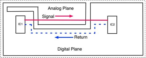
- Implementing separate power and ground planes for analog and digital sections
Grounding and Shielding
Proper grounding and shielding are essential for reducing radiated EMI in PCBs. Some best practices include:
- Using a solid ground plane to provide a low-impedance return path for high-frequency currents
- Implementing a star grounding scheme to minimize ground loops
- Using shielding cans or enclosures for sensitive components or high-noise sources
- Providing shielding for high-speed traces using coplanar waveguides or microstrip with ground fill
- Ensuring proper bonding and grounding of shielded connectors and cables
Signal Routing and Layer Stackup
Signal routing and layer stackup play a significant role in reducing radiated EMI. Key considerations include:
- Routing high-speed traces on inner layers between power and ground planes
- Using a symmetrical layer stackup to minimize EMI radiation
- Avoiding routing high-speed traces near board edges or over splits in power/ground planes
- Using differential pair routing for high-speed signals to minimize loop area and EMI
- Providing adequate spacing between high-speed traces and other signals
Component Placement and Orientation
Component placement and orientation can also impact radiated EMI. Some guidelines include:
- Placing decoupling capacitors as close to ICs as possible
- Orienting components to minimize loop areas and EMI coupling
- Avoiding placement of high-speed components near board edges or connectors
- Using shielding cans or enclosures for high-noise components
- Providing adequate spacing between components to minimize crosstalk and EMI coupling

Simulation and Testing for EMI
Simulation and testing are essential for identifying and mitigating EMI issues in high-speed, high-frequency PCBs. Some common techniques include:
- Electromagnetic simulation (EM simulation)
- Pre-compliance testing
- Full-compliance testing
Electromagnetic Simulation
EM simulation tools can help predict and analyze EMI performance of PCBs before fabrication. These tools can:
- Identify potential EMI sources and coupling paths
- Optimize component placement and routing for EMI reduction
- Evaluate the effectiveness of shielding and grounding techniques
- Predict the impact of design changes on EMI performance
Pre-Compliance Testing
Pre-compliance testing involves performing initial EMI measurements on the PCB to identify potential issues early in the design process. This can be done using:
- Spectrum analyzers and near-field probes to detect EMI hot spots
- TEM cells or anechoic chambers for radiated emissions testing
- Line impedance stabilization networks (LISNs) for conducted emissions testing
- Oscilloscopes and probes for time-domain measurements
Full-Compliance Testing
Full-compliance testing is the final step in verifying that the PCB meets the relevant EMI standards and regulations. This typically involves:
- Testing in a certified EMC laboratory
- Using calibrated antennas and receivers for radiated emissions measurements
- Performing conducted emissions tests using LISNs and EMI receivers
- Documenting test results and ensuring compliance with applicable standards
Best Practices for EMI Reduction in PCBs
To summarize, here are some best practices for reducing radiated EMI in high-speed, high-frequency PCBs:
- Minimize trace lengths and match impedances
- Use solid power and ground planes with proper decoupling
- Place decoupling capacitors close to ICs and use a mix of values
- Use shielded connectors and cables with proper termination
- Choose low-EMI oscillators and provide adequate shielding
- Implement partitioning and zoning in PCB layout
- Ensure proper grounding and shielding techniques
- Optimize signal routing and layer stackup for EMI reduction
- Consider component placement and orientation for minimal EMI coupling
- Perform EM simulations and pre-compliance testing to identify and mitigate EMI issues early
- Conduct full-compliance testing to ensure adherence to relevant EMI standards
By following these guidelines and best practices, designers can effectively minimize radiated EMI in high-speed, high-frequency PCBs, ensuring better signal integrity, performance, and compliance with regulatory requirements.
FAQ
Q1: What is the difference between radiated and conducted EMI?
A1: Radiated EMI refers to electromagnetic interference that is transmitted through the air as electromagnetic waves, while conducted EMI is interference that propagates through conductors, such as power lines, signal traces, or cables.
Q2: How does the rise/fall time of a signal affect radiated EMI?
A2: Faster rise and fall times of a signal result in higher-frequency harmonics, which are more likely to radiate EMI. Reducing the rise/fall times of high-speed signals can help minimize radiated EMI.
Q3: What is the purpose of a decoupling capacitor in EMI reduction?
A3: Decoupling capacitors help to minimize power supply noise and provide a local, low-impedance source of charge for ICs. By placing decoupling capacitors close to ICs and using a mix of capacitor values, designers can reduce high-frequency noise and minimize radiated EMI.
Q4: How can partitioning and zoning help reduce EMI in a PCB?
A4: Partitioning and zoning involve dividing the PCB into functional blocks and isolating them from each other using ground planes, guard traces, or separate power and ground planes. This helps to minimize EMI coupling between different sections of the PCB, reducing overall EMI emissions.
Q5: Why is full-compliance testing important for EMI verification?
A5: Full-compliance testing is the final step in verifying that a PCB meets the relevant EMI standards and regulations. It involves testing the PCB in a certified EMC laboratory using calibrated equipment and documenting the results to ensure compliance. Passing full-compliance testing is essential for products to be legally sold and used in their intended markets.
No responses yet