Introduction to QFP and QFN Packages
Quad Flat Package (QFP) and Quad Flat No-lead (QFN) are two popular surface-mount package types for integrated circuits (ICs). Both QFP and QFN packages offer advantages in terms of size, performance, and cost-effectiveness for various electronic applications. This article will provide an in-depth comparison of QFP and QFN packages, highlighting their key features, benefits, and differences.
What is a QFP Package?
A Quad Flat Package (QFP) is a surface-mount package with leads extending from all four sides of the package body. QFP packages are rectangular and have a flat profile, making them suitable for applications where space is limited. The leads are bent down and away from the package body, allowing for easy soldering to a printed circuit board (PCB).
What is a QFN Package?
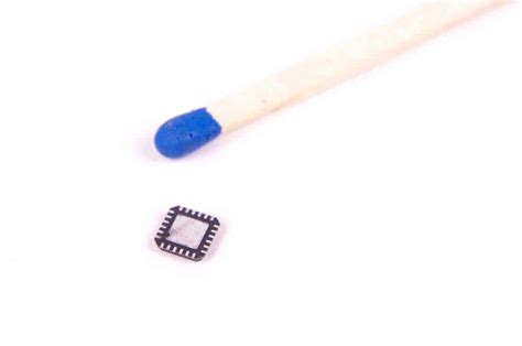
A Quad Flat No-lead (QFN) package is a surface-mount package that lacks the extended leads found in QFP packages. Instead, QFN packages have exposed pads on the bottom of the package that are used for soldering directly to a PCB. This design results in a smaller package size and improved thermal and electrical performance compared to QFP packages.
Key Features and Benefits of QFP Packages
Lead Configuration and Pitch
QFP packages have leads extending from all four sides of the package body. The number of leads can vary depending on the package size and the complexity of the IC. Common lead counts for QFP packages include 32, 44, 64, 80, 100, 120, 144, and 176.
The pitch, or the distance between the centers of adjacent leads, is an essential factor in determining the package size and the ease of PCB assembly. Common pitches for QFP packages include:
- 0.4 mm
- 0.5 mm
- 0.65 mm
- 0.8 mm
- 1.0 mm
Smaller pitches allow for higher lead counts and more compact package sizes but may require more advanced PCB assembly techniques.
Package Sizes and Dimensions
QFP packages come in various sizes to accommodate different IC designs and application requirements. Some common QFP package sizes include:
| Package Size | Dimensions (mm) | Typical Lead Count |
|---|---|---|
| QFP32 | 7 x 7 | 32 |
| QFP44 | 10 x 10 | 44 |
| QFP64 | 12 x 12 | 64 |
| QFP80 | 14 x 14 | 80 |
| QFP100 | 16 x 16 | 100 |
| QFP120 | 20 x 20 | 120 |
| QFP144 | 22 x 22 | 144 |
| QFP176 | 24 x 24 | 176 |
The package height is typically around 1.4 mm to 3.6 mm, depending on the lead count and package size.
Thermal Performance
QFP packages offer good thermal performance, allowing for efficient heat dissipation from the IC to the PCB. The exposed leads of the QFP package act as thermal paths, conducting heat away from the package body. However, the thermal performance of QFP packages is generally lower than that of QFN packages due to the limited contact area between the package and the PCB.
Ease of PCB Assembly
QFP packages are relatively easy to assemble on a PCB using standard surface-mount assembly techniques, such as solder paste printing, component placement, and reflow soldering. The extended leads of the QFP package provide a larger contact area for soldering, making the package more forgiving in terms of placement accuracy and solder joint formation.
However, as the lead pitch decreases, the assembly process becomes more challenging, requiring more precise solder paste printing and component placement to avoid short circuits or open connections.

Key Features and Benefits of QFN Packages
Pad Configuration and Pitch
QFN packages have exposed pads on the bottom of the package body, which are used for soldering directly to a PCB. The pads are typically arranged in a grid pattern, with a thermal pad in the center for improved heat dissipation. The number of pads can vary depending on the package size and the complexity of the IC, with common pad counts ranging from 12 to 100 or more.
The pitch of QFN packages is generally smaller than that of QFP packages, allowing for more compact package sizes. Common pitches for QFN packages include:
- 0.4 mm
- 0.5 mm
- 0.65 mm
Package Sizes and Dimensions
QFN packages are available in various sizes to suit different IC designs and application requirements. Some common QFN package sizes include:
| Package Size | Dimensions (mm) | Typical Pad Count |
|---|---|---|
| QFN16 | 3 x 3 | 16 |
| QFN24 | 4 x 4 | 24 |
| QFN32 | 5 x 5 | 32 |
| QFN48 | 6 x 6 | 48 |
| QFN64 | 8 x 8 | 64 |
| QFN100 | 10 x 10 | 100 |
The package height is typically around 0.8 mm to 1.0 mm, making QFN packages thinner than QFP packages.
Enhanced Thermal Performance
One of the key advantages of QFN packages is their excellent thermal performance. The exposed pad on the bottom of the package provides a direct thermal path from the IC to the PCB, allowing for efficient heat dissipation. The thermal pad is typically soldered to a corresponding thermal pad on the PCB, creating a low-resistance thermal interface.
The improved thermal performance of QFN packages enables higher power densities and better reliability compared to QFP packages, making them suitable for applications with high power requirements or operating in harsh environments.
Electrical Performance
QFN packages offer superior electrical performance compared to QFP packages. The shorter lead lengths and the absence of extended leads in QFN packages result in reduced parasitic inductance and capacitance, which can improve signal integrity and reduce electromagnetic interference (EMI).
The improved electrical characteristics of QFN packages make them well-suited for high-frequency applications, such as RF and wireless communication devices, where signal quality and low noise are critical.
PCB Assembly Challenges
While QFN packages offer many benefits, they also present some challenges for PCB assembly. The smaller pitch and the lack of extended leads in QFN packages require more precise solder paste printing and component placement to ensure proper solder joint formation and avoid short circuits or open connections.
Additionally, the exposed pad on the bottom of the QFN package can be prone to voiding during the soldering process, which can negatively impact the thermal and electrical performance of the package. Proper solder paste selection, stencil design, and reflow profile optimization are essential to mitigate these issues and achieve reliable solder joints.

Comparing QFP and QFN Packages
Size and Footprint
When comparing QFP and QFN packages of similar lead/pad counts, QFN packages typically have a smaller footprint than QFP packages. This size difference is due to the absence of extended leads in QFN packages, which allows for a more compact package design.
For example, a QFN48 package with a 6 mm x 6 mm footprint is significantly smaller than a QFP48 package with a 10 mm x 10 mm footprint. The smaller size of QFN packages makes them advantageous for space-constrained applications, such as mobile devices, wearables, and IoT sensors.
Thermal Performance Comparison
QFN packages generally offer better thermal performance than QFP packages. The exposed pad on the bottom of the QFN package provides a direct thermal path to the PCB, allowing for more efficient heat dissipation. In contrast, QFP packages rely on the extended leads for heat dissipation, which have a limited contact area with the PCB.
The improved thermal performance of QFN packages can be quantified using thermal resistance measurements, such as junction-to-case (ΘJC) and junction-to-board (ΘJB) thermal resistance. Lower thermal resistance values indicate better heat transfer from the IC to the package and the PCB.
For example, a QFN32 package may have a ΘJC of 20 K/W and a ΘJB of 10 K/W, while a QFP32 package may have a ΘJC of 30 K/W and a ΘJB of 20 K/W. These values suggest that the QFN package can dissipate heat more effectively than the QFP package, resulting in lower IC junction temperatures and improved reliability.
Electrical Performance Comparison
QFN packages offer better electrical performance than QFP packages due to their shorter lead lengths and reduced parasitic inductance and capacitance. The improved electrical characteristics of QFN packages can be particularly beneficial for high-frequency applications, where signal integrity and low noise are essential.
Some key electrical performance metrics to consider when comparing QFP and QFN packages include:
- Parasitic inductance: QFN packages have lower parasitic inductance than QFP packages, which can help reduce signal distortion and improve signal integrity.
- Parasitic capacitance: QFN packages have lower parasitic capacitance than QFP packages, which can help reduce signal crosstalk and improve high-frequency performance.
- Electromagnetic interference (EMI): The reduced lead lengths and improved shielding of QFN packages can help minimize EMI, making them suitable for applications with strict electromagnetic compatibility (EMC) requirements.
Cost Considerations
The cost comparison between QFP and QFN packages can vary depending on several factors, such as package size, lead/pad count, and production volume. In general, QFN packages tend to be more cost-effective than QFP packages for the following reasons:
-
Smaller package size: QFN packages have a smaller footprint than QFP packages, which allows for more packages to be manufactured on a single wafer or substrate. This increased packaging density can lead to lower per-unit costs.
-
Simplified package construction: QFN packages have a simpler construction than QFP packages, with no extended leads and fewer assembly steps. This simplicity can reduce manufacturing costs and improve production yields.
-
Reduced material usage: The absence of extended leads in QFN packages results in less material usage, such as copper and molding compound, compared to QFP packages. This reduced material consumption can contribute to lower package costs.
However, it is essential to consider the PCB assembly costs when evaluating the overall cost-effectiveness of QFP and QFN packages. The smaller pitch and more precise assembly requirements of QFN packages may result in higher PCB assembly costs compared to QFP packages. The cost impact of PCB assembly should be carefully assessed based on the specific application requirements, production volume, and available assembly capabilities.

FAQ
1. Can QFP packages be replaced with QFN packages in existing designs?
In many cases, QFP packages can be replaced with QFN packages in existing designs, provided that the PCB layout is modified to accommodate the different package footprint and pad configuration. However, the feasibility of such a replacement should be carefully evaluated based on the specific design requirements, such as thermal management, electrical performance, and assembly capabilities.
2. Are QFN packages suitable for high-reliability applications?
Yes, QFN packages can be suitable for high-reliability applications, provided that proper design and assembly practices are followed. The improved thermal performance and lower parasitic effects of QFN packages can contribute to enhanced reliability. However, the reliability of QFN packages in specific applications should be verified through thorough testing and qualification processes.
3. What are the challenges in soldering QFN packages?
The main challenges in soldering QFN packages include ensuring proper solder paste volume and placement accuracy, avoiding solder bridging between pads, and minimizing voiding in the thermal pad solder joint. These challenges can be addressed through careful stencil design, solder paste selection, and reflow profile optimization. Proper PCB layout and pad design can also help improve the soldering process and reliability of QFN packages.
4. How does the thermal performance of QFN packages compare to other package types?
QFN packages generally offer better thermal performance than QFP and other leadframe-based packages due to their exposed thermal pad and direct heat transfer path to the PCB. However, the thermal performance of QFN packages may be lower than that of some other package types, such as Ball Grid Array (BGA) packages, which have a larger number of solder balls and a more distributed heat transfer path. The choice of package type for a specific application should be based on a comprehensive evaluation of thermal requirements, cost, and other design factors.
5. Are there any limitations on the IC size that can be accommodated by QFN packages?
The maximum IC size that can be accommodated by QFN packages is primarily limited by the package dimensions and the number of pads available. Larger QFN packages, such as QFN100 or larger, can accommodate ICs with higher pin counts and larger die sizes. However, as the package size increases, the benefits of QFN packages in terms of size reduction and thermal performance may diminish compared to other package types, such as BGA packages. The choice of package size and type should be based on a careful consideration of the IC size, pin count, and other design requirements.
Conclusion
In conclusion, QFP and QFN packages are both widely used surface-mount packages for integrated circuits, each with its own set of advantages and limitations. QFP packages offer a robust and reliable solution with good thermal performance and ease of assembly, while QFN packages provide a more compact footprint, improved thermal and electrical performance, and cost-effectiveness.
When choosing between QFP and QFN packages for a specific application, engineers should carefully consider factors such as the required package size, thermal management, electrical performance, assembly capabilities, and cost. By understanding the key features and differences between these package types, designers can make informed decisions that optimize the performance, reliability, and cost-effectiveness of their electronic systems.
As technology continues to advance and the demand for smaller, more efficient, and high-performance electronic devices grows, the selection of appropriate packaging solutions will remain a critical aspect of electronic design. Both QFP and QFN packages are likely to continue evolving to meet the ever-changing requirements of the electronics industry, offering engineers a range of options to suit their specific application needs.
No responses yet