What is a Printed Wiring Board (PWB)?
A Printed Wiring Board (PWB) is a board that has conductive pathways or traces printed onto a non-conductive substrate. These traces are used to connect electronic components and create a functional circuit. The term “Printed Wiring Board” was coined in the early days of electronics manufacturing when the process involved printing wires onto a board.
History of PWBs
The concept of printed wiring can be traced back to the early 1900s when Albert Hanson, a German inventor, filed a patent for a method of printing conductive traces onto an insulating material. However, it wasn’t until the 1920s that the first practical application of printed wiring was developed by Charles Ducas, an American inventor.
Ducas’ method involved printing conductive ink onto a board and then electroplating the traces with copper to increase their conductivity. This process was used to create simple circuits for radios and other electronic devices.
During World War II, the demand for electronic equipment skyrocketed, and the printed wiring process was refined and standardized. The National Bureau of Standards (now known as the National Institute of Standards and Technology) published a set of guidelines for printed wiring in 1947, which helped to establish the term “Printed Wiring Board” as the standard terminology.
PWB Manufacturing Process
The manufacturing process for PWBs has evolved over the years, but the basic principles remain the same. The process typically involves the following steps:
- Designing the circuit layout using CAD software
- Printing the circuit pattern onto a photosensitive film
- Laminating the film onto a copper-clad board
- Exposing the board to UV light to harden the photosensitive material
- Etching away the unwanted copper to create the circuit traces
- Drilling holes for component leads and vias
- Applying a solder mask and silkscreen to protect the board and label components
Advantages of PWBs
PWBs offer several advantages over other types of circuit boards, including:
- Lower cost due to the simplicity of the manufacturing process
- Faster production times due to the ability to produce multiple boards simultaneously
- Improved reliability due to the elimination of manual wiring errors
- Increased flexibility in circuit design due to the ability to create complex trace patterns
What is a Printed Circuit Board (PCB)?
A Printed Circuit Board (PCB) is a more advanced version of a PWB that includes additional features such as multiple layers, through-hole components, and surface-mounted devices. PCBs are used in a wide range of electronic devices, from smartphones and laptops to medical equipment and aerospace systems.
History of PCBs
The term “Printed Circuit Board” was first used in the 1950s to describe boards that included printed components as well as printed wiring. However, it wasn’t until the 1960s that the term became widely adopted in the industry.
The development of PCBs was driven by the need for more complex and compact electronic devices. As the number of components in electronic devices increased, it became increasingly difficult to manually wire them together. PCBs allowed for the integration of multiple components onto a single board, reducing the size and complexity of electronic devices.
PCB Manufacturing Process
The manufacturing process for PCBs is similar to that of PWBs, but with some additional steps:
- Designing the circuit layout using CAD software
- Creating a multilayer stack-up of copper-clad boards
- Drilling holes for vias and component leads
- Plating the holes with copper to create conductive pathways between layers
- Etching away the unwanted copper to create the circuit traces
- Applying a solder mask and silkscreen to protect the board and label components
- Populating the board with components using automated assembly machines
Advantages of PCBs
PCBs offer several advantages over PWBs, including:
- Increased circuit density due to the ability to create multiple layers
- Improved signal integrity due to the use of controlled impedance traces
- Better heat dissipation due to the use of metal core substrates
- Enhanced reliability due to the use of surface-mounted components

PWB vs PCB: Technical Differences
While the terms PWB and PCB are often used interchangeably, there are some technical differences between the two:
| Feature | PWB | PCB |
|---|---|---|
| Layers | Single layer | Multiple layers |
| Components | Through-hole only | Through-hole and surface-mounted |
| Vias | Uncommon | Common |
| Trace Width | Wider | Narrower |
| Trace Spacing | Wider | Narrower |
| Solder Mask | Optional | Standard |
| Silkscreen | Optional | Standard |
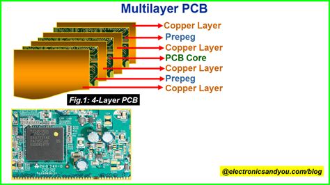
Layers
PWBs are typically single-layer boards, meaning that all of the conductive traces are on one side of the board. PCBs, on the other hand, can have multiple layers of conductive traces separated by insulating material. This allows for more complex circuit designs and higher component density.
Components
PWBs are limited to through-hole components, which have leads that are inserted into holes drilled in the board and soldered in place. PCBs can accommodate both through-hole and surface-mounted components, which are soldered directly onto the surface of the board. Surface-mounted components are smaller and can be placed more closely together, allowing for higher component density.
Vias
Vias are conductive pathways that connect traces on different layers of a PCB. They are created by drilling holes in the board and plating them with copper. Vias are uncommon in PWBs due to their single-layer design, but are a standard feature in PCBs.
Trace Width and Spacing
The width and spacing of the conductive traces on a PWB are typically wider than those on a PCB. This is due to the limitations of the printing process used to create PWBs. PCBs can have narrower traces and spacing, allowing for more complex circuit designs and higher component density.
Solder Mask and Silkscreen
Solder mask and silkscreen are optional features on PWBs, but are standard on PCBs. Solder mask is a coating that is applied to the board to protect the copper traces from oxidation and prevent solder bridges from forming between adjacent traces. Silkscreen is a printed layer that labels components and provides other important information about the board.

Which Term is Standard Usage?
In today’s industry, the term “Printed Circuit Board” (PCB) is considered standard usage. While the term “Printed Wiring Board” (PWB) is still used occasionally, it is more often used to refer specifically to single-layer boards without additional features such as solder mask and silkscreen.
The term PCB has become the preferred terminology for several reasons:
- It is more inclusive, encompassing both single-layer and multi-layer boards, as well as boards with surface-mounted components and other advanced features.
- It is more widely recognized and understood by professionals in the electronics industry.
- It is the term used in most industry standards and specifications, such as IPC (Association Connecting Electronics Industries) standards.

Frequently Asked Questions (FAQ)
1. Can a PWB have surface-mounted components?
No, PWBs are limited to through-hole components only. Surface-mounted components require a PCB with solder mask and other advanced features.
2. Are PCBs more expensive than PWBs?
Yes, PCBs are generally more expensive than PWBs due to their additional features and more complex manufacturing process. However, the cost difference has decreased over time as PCB manufacturing has become more automated and efficient.
3. Can a PCB have only one layer?
Yes, a PCB can have only one layer, but it is still considered a PCB rather than a PWB due to its other advanced features such as solder mask and silkscreen.
4. Are there any advantages to using a PWB over a PCB?
PWBs may be preferable in certain low-cost, low-complexity applications where the additional features of a PCB are not necessary. PWBs may also be used in prototyping or small-batch production where the cost of producing a PCB is not justified.
5. Are there any industry standards that still use the term PWB?
While most industry standards have transitioned to using the term PCB, there may be some older or specialized standards that still use the term PWB. However, these are becoming increasingly rare as the term PCB has become the accepted standard.
Conclusion
In conclusion, while the terms PWB and PCB are often used interchangeably, there are important technical differences between the two. PWBs are simpler, single-layer boards with through-hole components, while PCBs are more advanced boards with multiple layers, surface-mounted components, and other features such as solder mask and silkscreen.
In today’s industry, the term PCB is considered standard usage due to its inclusivity, recognizability, and use in industry standards. While PWBs may still have a place in certain low-cost or low-complexity applications, PCBs have become the preferred choice for most electronic devices due to their advanced features and capabilities.
As the electronics industry continues to evolve, it is likely that the term PCB will remain the standard terminology for the foreseeable future. However, it is important for professionals in the industry to be aware of the history and technical differences between PWBs and PCBs in order to effectively communicate and collaborate with colleagues and clients.
No responses yet