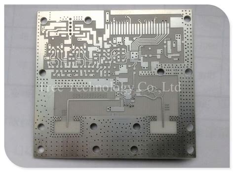
Introduction to PTH PCB
PTH PCB, or Plated Through Hole Printed Circuit Board, is a type of circuit board that features electroplated holes connecting different layers of the board. These holes, also known as vias, allow electrical signals to pass through the layers, enabling more complex circuit designs and improved electrical performance. PTH PCBs are widely used in various electronic devices, from consumer electronics to industrial equipment and aerospace applications.
How PTH PCBs are Manufactured
The manufacturing process of PTH PCBs involves several steps:
- Drilling: Holes are drilled into the bare PCB substrate according to the design specifications.
- Deburring: The drilled holes are cleaned and smoothed to remove any debris or rough edges.
- Electroless Copper Deposition: A thin layer of copper is chemically deposited onto the hole walls and the surface of the PCB.
- Electroplating: Additional copper is electroplated onto the electroless copper layer to achieve the desired thickness and ensure good conductivity.
- Photoresist Application: A photoresist layer is applied to the PCB surface and patterned using UV light exposure and development.
- Etching: The exposed copper areas are etched away, leaving the desired circuit pattern.
- Photoresist Removal: The remaining photoresist is stripped off, revealing the final copper circuit pattern.
- Surface Finishing: A protective surface finish, such as HASL (Hot Air Solder Leveling) or ENIG (Electroless Nickel Immersion Gold), is applied to the PCB to prevent oxidation and improve solderability.
Advantages of PTH PCB
PTH PCBs offer several advantages over other types of circuit boards:
- Mechanical Strength: The plated through holes provide additional mechanical support, making PTH PCBs more durable and resistant to vibration and shock.
- Electrical Reliability: The electroplated copper in the holes ensures a reliable electrical connection between layers, reducing the risk of signal loss or interference.
- High Current Carrying Capacity: PTH PCBs can handle higher current loads compared to surface mount technology (SMT) due to the larger cross-sectional area of the plated holes.
- Easier Assembly: Through-hole components are easier to install and inspect compared to surface-mount components, making PTH PCBs suitable for manual assembly or prototyping.
PTH PCB Design Considerations
When designing a PTH PCB, several factors must be taken into account to ensure optimal performance and manufacturability.
Hole Size and Spacing
The hole size and spacing are critical parameters in PTH PCB design. The hole diameter should be large enough to accommodate the component leads and allow for proper plating, but not too large to compromise the board’s structural integrity. The minimum hole size is typically 0.3mm, while the maximum size depends on the specific application and manufacturing capabilities.
The spacing between holes, also known as pad-to-pad clearance, should be sufficient to prevent short circuits and ensure reliable soldering. The minimum spacing is usually 0.2mm, but it may vary depending on the PCB manufacturer and the chosen surface finish.
Copper Thickness
The copper thickness in PTH PCBs is an essential factor in determining the current carrying capacity and signal integrity. Thicker copper layers can handle higher currents and provide better shielding against electromagnetic interference (EMI). However, increasing the copper thickness also increases the overall weight and cost of the PCB.
The standard copper thicknesses for PTH PCBs are:
| Copper Weight (oz) | Thickness (μm) |
|---|---|
| 0.5 | 17.5 |
| 1 | 35 |
| 2 | 70 |
| 3 | 105 |
| 4 | 140 |
Layer Stack-up
The layer stack-up refers to the arrangement of copper layers and insulating materials in a multi-layer PTH PCB. A proper layer stack-up ensures signal integrity, minimizes crosstalk, and provides adequate power and ground distribution.
A typical 4-layer PTH PCB stack-up might look like this:
| Layer | Material | Thickness (mm) |
|---|---|---|
| Top Copper | Copper | 0.035 |
| Prepreg | FR-4 | 0.2 |
| Inner Layer 1 | Copper | 0.035 |
| Core | FR-4 | 0.5 |
| Inner Layer 2 | Copper | 0.035 |
| Prepreg | FR-4 | 0.2 |
| Bottom Copper | Copper | 0.035 |
The prepreg and core materials provide insulation between the copper layers, while the copper layers themselves carry signals and power.
Via Types
Vias are the plated holes that connect different layers in a PTH PCB. There are several types of vias, each with its own characteristics and applications.
- Through Vias: These vias go through the entire thickness of the PCB, connecting all layers. They are the most common type of via and are used for component mounting and inter-layer connections.
- Blind Vias: Blind vias start from either the top or bottom layer and terminate at an inner layer. They are used to connect surface components to inner layers, saving space and improving signal routing.
- Buried Vias: Buried vias connect two or more inner layers without reaching the top or bottom layers. They are used to create complex interconnections between inner layers and are not visible from the surface of the PCB.
- Micro Vias: Micro vias are small-diameter vias (typically less than 0.15mm) used in high-density interconnect (HDI) PCBs. They enable finer pitch components and higher routing density.

PTH PCB Assembly
The assembly process for PTH PCBs involves soldering components to the board through the plated holes. There are two main methods for PTH PCB assembly: wave soldering and selective soldering.
Wave Soldering
Wave soldering is a process where the populated PCB is passed over a molten solder wave. The solder fills the plated through holes and creates a strong mechanical and electrical connection between the components and the board. Wave soldering is suitable for high-volume production and works well with through-hole components.
The wave soldering process consists of the following steps:
- Flux Application: A thin layer of flux is applied to the bottom side of the PCB to improve solder wettability and prevent oxidation.
- Preheating: The PCB is preheated to activate the flux and minimize thermal shock during soldering.
- Solder Wave Contact: The PCB is passed over the molten solder wave, which fills the plated holes and creates solder joints.
- Cooling: The soldered PCB is cooled to allow the solder joints to solidify.
- Cleaning: Any remaining flux residue is cleaned from the PCB surface.
Selective Soldering
Selective soldering is a process where solder is applied only to specific areas of the PCB, typically using a solder fountain or mini-wave. This method is suitable for mixed-technology PCBs that contain both through-hole and surface-mount components, or for boards with components that are sensitive to the high temperatures of wave soldering.
The selective soldering process involves the following steps:
- Flux Application: Flux is applied to the specific areas to be soldered.
- Preheating: The PCB is preheated to activate the flux and minimize thermal shock.
- Solder Application: Molten solder is applied to the targeted areas using a solder fountain or mini-wave.
- Cooling: The soldered areas are cooled to allow the solder joints to solidify.
- Cleaning: Any remaining flux residue is cleaned from the PCB surface.

Testing and Quality Control
After assembly, PTH PCBs undergo various testing and quality control procedures to ensure their functionality, reliability, and compliance with industry standards.
Automated Optical Inspection (AOI)
AOI is a non-contact inspection method that uses cameras and image processing software to detect visible defects on the PCB surface, such as missing components, solder bridges, or incorrect component placement. AOI is a fast and efficient way to identify assembly issues early in the production process.
In-Circuit Testing (ICT)
ICT is a test method that verifies the proper assembly and functionality of individual components on the PCB. ICT uses a bed-of-nails fixture to make electrical contact with the board and perform measurements such as resistance, capacitance, and voltage. This test helps identify faulty components or assembly errors that may not be visible during optical inspection.
Functional Testing
Functional testing involves powering up the assembled PCB and verifying its operation under real-world conditions. This test ensures that the PCB performs as intended and meets the specified requirements. Functional testing may include temperature cycling, vibration testing, or electromagnetic compatibility (EMC) testing, depending on the application and industry standards.

Applications of PTH PCB
PTH PCBs find applications in a wide range of industries and products, such as:
- Consumer Electronics: Televisions, home appliances, and audio equipment often use PTH PCBs for their power supply and control boards.
- Industrial Controls: PTH PCBs are used in industrial control systems, such as programmable logic controllers (PLCs) and human-machine interfaces (HMIs), due to their reliability and resistance to harsh environments.
- Automotive Electronics: PTH PCBs are used in various automotive systems, including engine control units, infotainment systems, and power distribution modules.
- Medical Devices: Medical equipment, such as patient monitors and diagnostic devices, rely on PTH PCBs for their reliability and ability to handle high-current applications.
- Aerospace and Defense: PTH PCBs are used in avionics systems, satellites, and military equipment due to their mechanical strength and resistance to vibration and shock.
Frequently Asked Questions (FAQ)
-
Q: What is the difference between a PTH PCB and an SMT PCB?
A: A PTH PCB uses plated through holes to connect components and different layers of the board, while an SMT PCB uses surface-mounted components that are soldered directly onto the board surface. PTH PCBs offer better mechanical strength and higher current carrying capacity, while SMT PCBs enable higher component density and faster assembly. -
Q: Can PTH and SMT components be used on the same PCB?
A: Yes, mixed-technology PCBs that combine both PTH and SMT components are common. These boards leverage the advantages of both technologies, using PTH for high-current or mechanically demanding components and SMT for high-density and high-speed components. -
Q: What is the minimum hole size for a PTH PCB?
A: The minimum hole size for a PTH PCB is typically 0.3mm, but it may vary depending on the specific manufacturing capabilities and design requirements. Smaller hole sizes are possible with advanced manufacturing techniques, such as micro-vias in HDI PCBs. -
Q: How does the copper thickness affect the performance of a PTH PCB?
A: Thicker copper layers in a PTH PCB can handle higher currents and provide better shielding against electromagnetic interference (EMI). However, increasing the copper thickness also increases the overall weight and cost of the PCB. The appropriate copper thickness should be selected based on the specific application requirements and design constraints. -
Q: What are the common surface finishes for PTH PCBs?
A: Common surface finishes for PTH PCBs include Hot Air Solder Leveling (HASL), Electroless Nickel Immersion Gold (ENIG), and Immersion Silver (ImAg). The choice of surface finish depends on factors such as solderability, shelf life, and compatibility with the assembly process and operating environment.
Conclusion
PTH PCBs are a reliable and widely used type of circuit board that offer numerous advantages, such as mechanical strength, electrical reliability, and high current carrying capacity. By understanding the design considerations, manufacturing process, and assembly techniques for PTH PCBs, engineers and manufacturers can create high-quality boards that meet the demands of various industries and applications.
As technology advances, PTH PCBs continue to evolve, with improvements in materials, manufacturing processes, and testing methods. By staying up-to-date with the latest developments and best practices in PTH PCB design and manufacturing, companies can ensure the production of reliable, high-performance electronic devices that meet the ever-increasing demands of the modern world.
No responses yet