Introduction to PCB Layout
Printed Circuit Board (PCB) layout is a crucial step in the electronic design process. It involves arranging electronic components and routing the connections between them on a non-conductive substrate. The goal is to create a functional, reliable, and manufacturable board that meets the design requirements. PCB layout software plays a vital role in this process, providing designers with the tools they need to efficiently create and optimize their board layouts.
The Importance of PCB Layout Software
PCB layout software is essential for several reasons:
- Efficiency: It streamlines the design process, allowing designers to create complex layouts quickly and accurately.
- Accuracy: The software ensures that the layout adheres to design rules and constraints, minimizing errors and reducing the risk of manufacturing issues.
- Collaboration: Many PCB layout tools enable seamless collaboration between design teams, facilitating efficient communication and reducing design time.
- Optimization: Advanced features like auto-routing and design rule checking help optimize the layout for performance, reliability, and manufacturability.
Key Features of PCB Layout Software
When choosing a PCB layout software, consider the following key features:
Schematic Capture
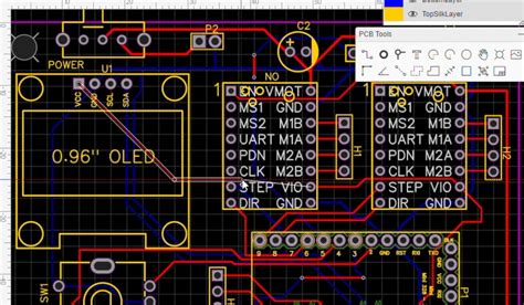
Schematic capture is the process of creating a graphical representation of the electronic circuit. It involves placing components and defining their connections. A good PCB layout software should have a robust schematic capture tool that allows designers to easily create and modify schematics.
Component Libraries
Component libraries are databases that contain information about electronic components, including their symbols, footprints, and properties. A comprehensive component library is essential for efficient PCB design, as it allows designers to quickly select and place components without having to create them from scratch.
Routing Tools
Routing is the process of connecting components on the PCB using conductive traces. PCB layout software should provide a range of routing tools, including manual and auto-routing options. Auto-routing algorithms can significantly speed up the routing process, while manual routing gives designers more control over critical connections.
Design Rule Checking (DRC)
Design Rule Checking (DRC) is a feature that automatically checks the layout against a set of predefined design rules. These rules ensure that the layout meets manufacturing requirements and industry standards. DRC helps identify and resolve issues early in the design process, reducing the risk of costly manufacturing errors.
3D Visualization
Many PCB layout tools offer 3D visualization capabilities, allowing designers to view their boards from different angles and identify potential mechanical issues. This feature is particularly useful for designs with complex mechanical requirements or tight space constraints.
Popular PCB Layout Software
There are several popular PCB layout software options available, each with its own strengths and weaknesses. Here are a few notable examples:
Altium Designer
Altium Designer is a comprehensive PCB design platform that offers schematic capture, PCB layout, and 3D visualization tools. It is known for its advanced features, such as multi-board design and real-time collaboration. Altium Designer is widely used in the industry and is suitable for complex, high-speed designs.
KiCad
KiCad is a free and open-source PCB design suite that includes schematic capture, PCB layout, and 3D visualization tools. It has a large and active community of users and developers, which ensures regular updates and improvements. KiCad is a great choice for hobbyists, students, and small businesses looking for a cost-effective solution.
Eagle
Eagle is a popular PCB design software that offers schematic capture, PCB layout, and auto-routing capabilities. It has a user-friendly interface and a large component library, making it a good choice for beginners and small-scale projects. Eagle is available in both free and paid versions, with the paid version offering additional features and support.
OrCAD
OrCAD is a powerful PCB design platform that includes schematic capture, PCB layout, and simulation tools. It is known for its advanced constraint management and design reuse capabilities, making it suitable for complex, high-speed designs. OrCAD is widely used in the industry and offers a range of extensions and integrations with other design tools.

PCB Layout Design Tips
Creating a successful PCB layout requires careful planning and attention to detail. Here are some tips to help you optimize your designs:
- Start with a good schematic: Ensure that your schematic is well-organized, properly annotated, and free of errors before starting the layout process.
- Plan your component placement: Arrange components logically, considering factors like signal flow, thermal management, and mechanical constraints.
- Use a grid: Aligning components and traces to a grid can help create a cleaner, more organized layout.
- Minimize trace lengths: Keep critical signal traces as short as possible to reduce noise, crosstalk, and signal integrity issues.
- Consider manufacturability: Follow the manufacturing guidelines provided by your PCB fabricator to ensure that your design is manufacturable and cost-effective.
Prototype Board Manufacturing
Once the PCB layout is complete, the next step is to manufacture a prototype board for testing and validation. There are several factors to consider when choosing a PCB manufacturer:
Capabilities
Ensure that the manufacturer has the capabilities to produce your specific design, including the required layer count, material, and finish.
Quality
Look for manufacturers with a proven track record of producing high-quality boards. Request sample boards or references from previous clients to assess their quality.
Turnaround Time
Consider the manufacturer’s turnaround time, especially if you are working on a tight deadline. Some manufacturers offer expedited services for an additional fee.
Cost
Get quotes from multiple manufacturers and compare their prices. Keep in mind that the lowest price may not always be the best option, as quality and reliability are crucial factors.
Frequently Asked Questions (FAQ)
-
What is the difference between schematic capture and PCB layout?
Schematic capture involves creating a graphical representation of the electronic circuit, while PCB layout involves arranging the components and routing the connections on a physical board. -
Do I need to know how to code to use PCB layout software?
No, most PCB layout software has a graphical user interface that allows designers to create layouts without coding knowledge. However, some advanced features may require scripting or programming skills. -
Can I create multi-layer PCBs with prototype board layout software?
Yes, most PCB layout software supports the design of multi-layer boards. The specific capabilities may vary depending on the software and version. -
How do I ensure that my PCB layout is manufacturable?
To ensure manufacturability, follow the design guidelines provided by your PCB fabricator, use DRC to catch potential issues, and consider factors like trace width, spacing, and hole sizes. -
What file formats are used for PCB layout?
Common file formats for PCB layout include Gerber (RS-274X), ODB++, and IPC-2581. These formats are used to transfer design data to PCB manufacturers for fabrication.
Conclusion
Prototype board layout software is an essential tool for creating efficient, accurate, and manufacturable PCB designs. By leveraging the key features of these tools, such as schematic capture, component libraries, routing tools, and DRC, designers can streamline the design process and create high-quality boards.
When selecting a PCB layout software, consider factors like your design requirements, budget, and experience level. Popular options include Altium Designer, KiCad, Eagle, and OrCAD, each with its own strengths and weaknesses.
To optimize your PCB layouts, start with a well-organized schematic, plan your component placement carefully, use a grid, minimize trace lengths, and consider manufacturability. When it comes to prototype board manufacturing, choose a reliable manufacturer with the capabilities, quality, turnaround time, and cost that meet your needs.
By following these guidelines and leveraging the power of prototype board layout software, you can create successful PCB designs that bring your electronic projects to life.
No responses yet