Introduction to PCB ESD Protection
Electrostatic discharge (ESD) is a sudden flow of electricity between two electrically charged objects. It can cause damage to sensitive electronic components on printed circuit boards (PCBs). Transient voltage suppressors (TVS) are devices used to protect PCBs from the damaging effects of ESD. In this article, we’ll dive deep into PCB ESD protection using TVS devices.
What is ESD and Why is PCB Protection Important?
ESD occurs when there is a buildup of static electricity between two objects at different electrical potentials. When these objects come into contact or close proximity, the electrical charge rapidly equalizes, causing a high voltage “spark.”
For PCBs, ESD can happen in a few ways:
– Human body model (HBM) – static discharge from a person
– Charged device model (CDM) – when a PCB itself is charged and contacts ground
– Machine model (MM) – discharge from assembly equipment to PCB
Even relatively small ESD events in the 100s of volts range can damage sensitive PCB components like ICs. Larger discharges in the kilovolt range can completely destroy parts.
Some negative effects of ESD on PCBs include:
– Latent damage – weakened/degraded parts that fail prematurely
– Immediate dielectric breakdown
– Thermal damage from arcing
– Blown fuses and damaged connectors
To prevent ESD problems, it’s crucial to incorporate proper PCB protection measures in the design stage. TVS diodes and related components are the most common and effective solution.
How Do Transient Voltage Suppressors (TVS) Work?
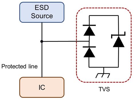
A TVS is a clamping device that limits voltage spikes by conducting current once a certain threshold is exceeded. It has a very high resistance at normal operating voltages but rapidly switches to a low resistance state when a transient overvoltage occurs, safely shunting excess current.
The most common type of TVS is an avalanche diode, which is like a Zener diode optimized for transient suppression rather than voltage regulation. During an ESD event, the TVS clamps the voltage across its terminals to a specified level, absorbing the transient energy and protecting the PCB circuitry.
Key attributes of TVS devices include:
– Standoff voltage (Vs) – max voltage before clamping activates
– Breakdown voltage (Vbr) – voltage at which TVS starts conducting
– Clamping voltage (Vc) – max voltage let through to circuit
– Peak pulse current (Ipp) – maximum transient current rating
– Joule rating – amount of transient energy absorption
There are both unidirectional and bidirectional TVS diodes. Unidirectional ones suppress spikes in one direction like a regular diode. Bidirectional TVS clamps work in both directions, conducting when the voltage exceeds the breakdown rating in either polarity.

TVS Device Options and Characteristics
TVS diodes come in various types and packages for different PCB protection needs. Two major categories are surface mount (SMT) and through-hole. Here’s a table summarizing common options:
| TVS Type | Package | Typical Ratings | Applications |
|---|---|---|---|
| SMT diode | SOD-923, 0201 | Vs: 3.3-18V, Ipp: 3-30A, 0.1-0.5J | High speed data lines, mobile devices |
| SMT diode array | SOT-23, SOT-143 | Vs per I/O: 3.3-18V, Ipp: 3-30A, 0.1-0.5J | I/O port protection |
| SMT polymer ESD | 0402, 0201 | 15-30kV HBM, pF capacitance | RF/high freq, touchscreens |
| Thru-hole diode | DO-35, DO-41 | Vs: 3.3-440V, Ipp: 3-10kA, 50-15kJ | Power lines, coax, high exposure |
| Thru-hole gas discharge tube (GDT) | 4-12mm diameter | 75-600V spark-over, 3-40kA, >5kJ | Telecom, AC mains, antennas |
Important characteristics to consider when selecting a TVS include:
1. Operating/standoff voltage – pick Vs higher than circuit Vmax
2. Clamping voltage – low Vc for better protection
3. Peak current and energy rating – handles expected threat level
4. Capacitance – minimal for high-speed signals
5. Leakage current – low to avoid adding load
6. Size – minimal, based on power handling needs
7. Configuration – bidirectional or unidirectional
8. Array options – multi-channel for I/O ports
9. Cost – balance with robustness required
Selecting and Placing TVS for Optimal PCB Protection
For maximum effectiveness, TVS devices should be placed as close as possible to the entry points of potential ESD on a PCB – I/O connectors, power inputs, exposed conductors, etc.
General guidelines for optimal TVS placement include:
– Position < 10mm from protected line if possible
– Minimize distance and loops between protected line and TVS
– Use dedicated low-Z GND connection for TVS
– Place upstream of and close to sensitive components
– Consider spacing multiple TVS along long signal lines
It’s also important to assess the expected exposure level of the end application and choose TVS ratings accordingly. IEC 61000-4-2 specifies standard ESD immunity test levels:
| Contact Discharge | Air Discharge |
|---|---|
| 2kV | 2kV |
| 4kV | 4kV |
| 6kV | 8kV |
| 8kV | 15kV |
For most consumer electronics, 8kV contact/15kV air is sufficient. Industrial and automotive may need 25kV+ air rating.
Additionally, consider the data rate and capacitive loading of signals to be protected. High-speed interfaces like USB 3.0 need TVS with minimal capacitance (<0.2pF) to avoid signal degradation.
Here is an example of TVS selection and placement on a basic PCB design with external I/O:
        TVS Array
       +---------+
I/O ---| I/O I/O |--- MCU
       +---------+
         | | | |
        GND GND GND
- Fast response SMT TVS array positioned close to I/O connector
- Protected lines have short distance to TVS with no stubs/branches
- TVS array internally connected to ground plane with minimal inductance
- Ratings: 5V standoff per I/O, 30kV air HBM, 0.5pF channel capacitance
PCB Layout Techniques for ESD Robustness
In addition to proper TVS usage, good PCB layout practices enhance ESD protection:
- Minimize loops/apertures that can inductively couple ESD
- Avoid long signal traces and unshielded conductors
- Use ground planes and guard rings around sensitive traces
- Maintain spacing between high-speed signals
- Follow controlled impedance routing guidelines
- Optimize placement of connectors, switches, buttons for minimal ESD exposure
- Keep unrelated signals away from ESD susceptible lines
Proper grounding techniques are particularly important for ESD. A low-impedance ground return path for TVS devices is critical. Some tips:
- Use dedicated GND via for each TVS device to PCB inner ground plane
- Minimize distance between TVS ground pin and GND via
- Avoid daisy-chaining grounds between multiple TVS
- Tie ESD grounds to chassis/earth ground where possible
- Use grounded shielding on cables and around exposed PCB edges
Putting it All Together – PCB ESD Protection Design Checklist
To summarize, here is a checklist for incorporating ESD protection in PCB designs:
- Identify all potential ESD entry points – connectors, switches, etc.
- Determine expected ESD exposure level (HBM voltage)
- Place TVS close to ESD entry points (<10mm)
- Select TVS standoff higher than circuit operating voltage
- Match TVS clamping specs to expected threat level
- Minimize capacitive loading, especially on high-speed signals
- Use bidirectional or unidirectional TVS as needed
- Consider multi-channel TVS arrays for I/O ports
- Minimize loop areas and distance between TVS and signal lines
- Route protected signals away from other traces
- Connect TVS grounds directly to PCB Ground Planes
- Add ground planes, guard rings for sensitive signals
- Optimize component placement for minimal ESD risk
- Use shielding on cables and exposed board areas
By following this systematic approach and leveraging proper TVS devices, PCB designers can effectively mitigate ESD risks, improving reliability and reducing costly failures and warranty claims.
FAQ on PCB ESD Protection
What is the most common failure mode for PCBs exposed to ESD?
Dielectric breakdown of IC inputs is the leading cause of ESD failures on PCBs. The extremely fast rise time and high voltage of ESD events can exceed the gate oxide breakdown rating of many ICs, causing permanent damage.
How much capacitance do TVS diodes add to a signal line?
The added capacitive load depends on the TVS technology and size. Lower capacitance TVS in small SMT packages can contribute <0.5pF which is suitable for many high-speed lines. Higher power rated devices may add a few pF. Consult datasheets.
Can a TVS be used to protect against lightning strikes?
Not solely. Lightning is a much higher power surge/transient event. TVS can be part of a multi-stage protection scheme in outdoor applications but additional GDTs, high energy varistors (MOVs) or spark gaps are typically needed.
Is it possible to simulate the impact of ESD on PCBs?
Yes, circuit simulators like HSpice and LTSPICE can model ESD events using the human body model (HBM) and charged device model (CDM) equivalent circuits. This allows designers to virtually assess the ESD susceptibility of PCBs and validate protection schemes.
Are there any PC board materials that are particularly good for ESD prevention?
While most standard FR-4 PCB material is adequate for ESD-sensitive designs, there are some higher performance laminate options. Isola 370HR and Rogers 4350B are two hydrocarbon ceramic laminates that offer improved dielectric properties and lower moisture absorption which can benefit ESD robustness.
No responses yet