What is PCB Assembly?
PCB assembly is the process of attaching electronic components to a printed circuit board (PCB) to create a functional electronic device. The PCB serves as the foundation for the electronic device, providing both mechanical support and electrical connectivity for the components. The assembly process involves a series of steps, including solder paste application, component placement, soldering, and inspection.
Types of PCB Assembly
There are two main types of PCB assembly:
-
Through-hole assembly (THA): This method involves inserting component leads through holes drilled in the PCB and soldering them to pads on the opposite side of the board.
-
Surface mount assembly (SMA): This technique involves placing components directly onto pads on the surface of the PCB and soldering them in place.
| Assembly Type | Advantages | Disadvantages |
|---|---|---|
| Through-hole | – Stronger mechanical bonds – Easier to replace components – Better for high-power applications |
– Larger component size – Higher assembly costs – Limited board space |
| Surface mount | – Smaller component size – Lower assembly costs – Higher component density |
– Weaker mechanical bonds – More difficult to replace components – Requires specialized equipment |
PCB Assembly Technology
Solder Paste Application
Solder paste, a mixture of tiny solder particles and flux, is applied to the PCB pads using a stencil or screen printing process. The stencil is aligned with the PCB, and solder paste is spread across the stencil, filling the holes that correspond to the component pads.
Component Placement
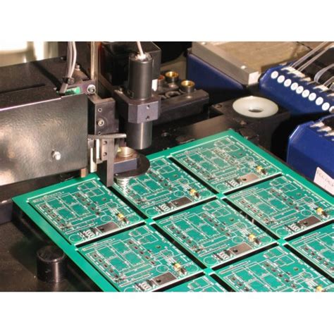
Components are placed onto the PCB using automated pick-and-place machines or by hand for low-volume or prototype assemblies. The machines use computer-aided design (CAD) files to determine the correct placement of each component.
Soldering
After component placement, the PCB undergoes a soldering process to create electrical connections between the components and the board. There are two primary soldering methods:
-
Reflow soldering: This method is used for surface mount components. The PCB is heated in a reflow oven, causing the solder paste to melt and form a permanent bond between the components and the board.
-
Wave soldering: This technique is used for through-hole components. The PCB is passed over a molten solder wave, which creates a solder joint between the component leads and the PCB pads.
Inspection and Testing
After soldering, the assembled PCB undergoes various inspection and testing procedures to ensure proper functionality and quality. These may include:
- Visual inspection
- Automated optical inspection (AOI)
- X-ray inspection
- In-circuit testing (ICT)
- Functional testing

Uses of PCB Assembly
PCB assembly is used in a wide range of industries and applications, including:
- Consumer electronics (smartphones, computers, televisions)
- Automotive electronics (engine control units, infotainment systems, sensors)
- Medical devices (pacemakers, imaging equipment, diagnostic tools)
- Aerospace and defense (avionics, communications systems, weapons systems)
- Industrial automation (PLCs, sensors, control panels)

Frequently Asked Questions (FAQ)
1. What is the difference between PCB fabrication and PCB assembly?
PCB fabrication is the process of manufacturing the bare printed circuit board, while PCB assembly involves attaching electronic components to the fabricated board to create a functional electronic device.
2. What are the advantages of using surface mount technology (SMT) in PCB assembly?
SMT offers several advantages, including smaller component sizes, lower assembly costs, and higher component density compared to through-hole technology. This allows for more compact and efficient electronic devices.
3. What is the purpose of solder paste in PCB assembly?
Solder paste serves two primary functions in PCB assembly. First, it contains the solder particles that create the electrical and mechanical connections between components and the PCB. Second, the flux in the solder paste helps to remove oxidation and improve solder wetting during the soldering process.
4. What is the role of pick-and-place machines in PCB assembly?
Pick-and-place machines are automated systems that place electronic components onto the PCB during the assembly process. They use computer-aided design (CAD) files to determine the correct placement of each component, ensuring precision and accuracy in the assembly process.
5. What types of testing are performed on assembled PCBs to ensure quality and functionality?
Assembled PCBs undergo various testing procedures, including visual inspection, automated optical inspection (AOI), X-ray inspection, in-circuit testing (ICT), and functional testing. These tests help to identify any defects or issues with the assembled board, ensuring that the final product meets the required quality standards and functions as intended.

No responses yet