Introduction to PCB Design for Manufacturing (DFM)
Designing printed circuit boards (PCBs) involves much more than just creating a schematic and laying out the board. To ensure your PCB design can be manufactured reliably and cost-effectively, it’s crucial to follow design for manufacturing (DFM) guidelines. DFM is the process of designing products with manufacturing in mind, taking into account the capabilities and limitations of the manufacturing processes involved.
In PCB design, DFM is essential to avoid manufacturing issues that can lead to delays, increased costs, or even non-functional boards. By understanding and preventing the most common DFM errors, you can streamline your PCB design process and ensure a smoother transition to manufacturing.
Top DFM Errors to Avoid in PCB Design
1. Incorrect Trace Width and Spacing
One of the most common DFM errors in PCB design is using incorrect trace widths and spacing. Traces that are too thin or too close together can cause manufacturing issues such as open circuits, short circuits, or signal integrity problems.
To prevent this error, follow these guidelines:
- Use appropriate trace widths based on the current carrying requirements and the PCB manufacturing capabilities
- Maintain sufficient spacing between traces, especially for high-voltage or high-frequency signals
- Consider the PCB material and layer stack-up when determining trace width and spacing
| Signal Type | Recommended Trace Width | Minimum Spacing |
|---|---|---|
| Digital | 0.2 mm – 0.4 mm | 0.2 mm |
| Analog | 0.3 mm – 0.6 mm | 0.3 mm |
| Power | 0.5 mm – 2.0 mm | 0.5 mm |
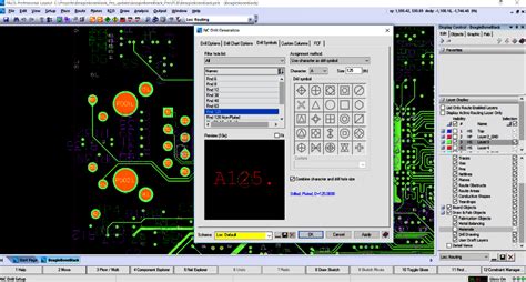
2. Incorrect Drill Sizes and Pad Sizes
Another common DFM error is using incorrect drill sizes or pad sizes for through-hole components or vias. If the drill size is too small, it can be difficult or impossible to properly plate the hole, leading to poor electrical connections. If the pad size is too small, it can cause issues with soldering or component placement.
To prevent this error, follow these guidelines:
- Use standard drill sizes that are compatible with the PCB manufacturer’s capabilities
- Ensure the pad size is appropriate for the component lead or via size
- Consider the PCB thickness when selecting drill sizes and pad sizes
| Drill Size | Minimum Pad Size |
|---|---|
| 0.2 mm | 0.6 mm |
| 0.3 mm | 0.7 mm |
| 0.4 mm | 0.8 mm |
| 0.5 mm | 0.9 mm |
3. Incorrect Solder Mask and Silkscreen
Solder mask and silkscreen are important elements of a PCB that help with component placement and soldering. However, incorrect solder mask or silkscreen can lead to manufacturing issues or assembly errors.
To prevent this error, follow these guidelines:
- Ensure solder mask openings are slightly larger than the pad size to allow for proper soldering
- Provide sufficient clearance between solder mask openings and adjacent components or traces
- Use clear and legible silkscreen labels for component placement and orientation
- Avoid placing silkscreen over pads or exposed copper areas
4. Incorrect Component Footprints
Using incorrect component footprints is another common DFM error that can cause issues with component placement and soldering. If the footprint is too small or the wrong shape, it can be difficult or impossible to properly place and solder the component.
To prevent this error, follow these guidelines:
- Use component footprints that match the actual component dimensions and lead spacing
- Verify the footprint dimensions against the component datasheet
- Consider the component height and orientation when designing the footprint
- Use standard footprints whenever possible to ensure compatibility with the PCB manufacturer’s capabilities
5. Lack of Design Rule Checking (DRC)
Design Rule Checking (DRC) is an essential step in the PCB design process that helps identify and prevent design errors. Failing to perform DRC or ignoring DRC warnings can lead to manufacturing issues or non-functional boards.
To prevent this error, follow these guidelines:
- Use DRC tools provided by your PCB design software to check for design errors
- Set up DRC rules based on the PCB manufacturer’s capabilities and requirements
- Review and address all DRC warnings before finalizing the design
- Perform a final DRC check before sending the design files to the manufacturer

PCB-DFM-Prevention Best Practices
In addition to avoiding the top DFM errors, there are several best practices you can follow to ensure your PCB design is optimized for manufacturing:
1. Communicate with Your PCB Manufacturer
Effective communication with your PCB manufacturer is crucial for ensuring a smooth transition from design to manufacturing. Share your design files, requirements, and any special considerations with the manufacturer early in the process. They can provide valuable feedback and guidance on DFM best practices specific to their capabilities.
2. Use Standard Components and Materials
Using standard components and materials whenever possible can help reduce manufacturing costs and lead times. Standard components are more readily available and are often less expensive than custom or specialized components. Similarly, using standard PCB materials and layer stack-ups can streamline the manufacturing process and reduce the risk of issues.
3. Design for Assembly (DFA)
In addition to designing for manufacturing, it’s important to consider the assembly process when designing your PCB. Design for Assembly (DFA) involves designing the PCB to facilitate easy and efficient assembly of components. Some DFA best practices include:
- Providing sufficient clearance around components for placement and soldering
- Using standard component packages and footprints
- Minimizing the number of unique components and orientations
- Clearly labeling components and pin 1 indicators
4. Perform Design Reviews
Conducting design reviews throughout the PCB design process can help identify and prevent potential DFM issues early on. Involve stakeholders from different disciplines, such as electrical engineering, mechanical engineering, and manufacturing, to ensure all aspects of the design are considered. Use design review checklists to systematically review the design for DFM compliance.
5. Use 3D Modeling and Simulation
Using 3D modeling and simulation tools can help visualize the PCB design and identify potential issues before manufacturing. 3D models can be used to check for component clearances, mechanical interferences, and thermal management. Simulation tools can be used to analyze signal integrity, power integrity, and electromagnetic compatibility (EMC) performance.

FAQ
- What is Design for Manufacturing (DFM) in PCB design?
Design for Manufacturing (DFM) in PCB design is the process of designing a printed circuit board with the manufacturing process in mind. It involves following guidelines and best practices to ensure the PCB can be manufactured reliably and cost-effectively.
- Why is DFM important in PCB design?
DFM is important in PCB design because it helps prevent manufacturing issues that can lead to delays, increased costs, or non-functional boards. By designing with manufacturing in mind, you can streamline the PCB design process and ensure a smoother transition to manufacturing.
- What are some common DFM errors in PCB design?
Some common DFM errors in PCB design include incorrect trace width and spacing, incorrect drill sizes and pad sizes, incorrect solder mask and silkscreen, incorrect component footprints, and lack of Design Rule Checking (DRC).
- How can I prevent DFM errors in my PCB design?
To prevent DFM errors in your PCB design, follow best practices such as communicating with your PCB manufacturer, using standard components and materials, designing for assembly (DFA), performing design reviews, and using 3D modeling and simulation tools.
- What is the role of Design Rule Checking (DRC) in PCB-DFM-Prevention?
Design Rule Checking (DRC) is an essential step in PCB-DFM-Prevention that helps identify and prevent design errors. By setting up DRC rules based on the PCB manufacturer’s capabilities and requirements, and reviewing and addressing all DRC warnings before finalizing the design, you can ensure your PCB design is optimized for manufacturing.

Conclusion
Preventing top DFM errors in your PCB design is crucial for ensuring a successful and cost-effective manufacturing process. By understanding and avoiding common errors such as incorrect trace width and spacing, incorrect drill sizes and pad sizes, incorrect solder mask and silkscreen, incorrect component footprints, and lack of Design Rule Checking (DRC), you can minimize the risk of manufacturing issues and delays.
Following PCB-DFM-Prevention best practices, such as communicating with your PCB manufacturer, using standard components and materials, designing for assembly (DFA), performing design reviews, and using 3D modeling and simulation tools, can further optimize your PCB design for manufacturing.
By prioritizing DFM in your PCB design process, you can streamline the transition from design to manufacturing, reduce costs, and improve the overall quality and reliability of your printed circuit boards.

No responses yet