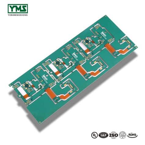
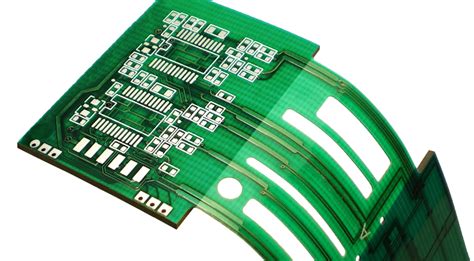
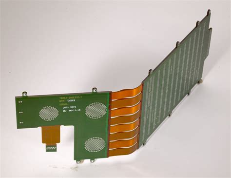
Introduction to Rigid-Flex PCBs
Rigid-flex PCBs are a unique type of printed circuit board that combines the benefits of both rigid and flexible PCBs. These boards consist of rigid PCB sections connected by flexible PCB sections, allowing for three-dimensional packaging and improved reliability in applications that require flexibility or space savings.
Advantages of Rigid-Flex PCBs
- Reduced weight and size
- Improved reliability
- Enhanced electrical performance
- Increased design flexibility
- Cost-effective for high-volume production
Applications of Rigid-Flex PCBs
Rigid-flex PCBs are used in a wide range of industries, including:
- Aerospace and defense
- Medical devices
- Consumer electronics
- Automotive electronics
- Industrial automation
Documenting Rigid-Flex PCBs for Manufacturing
Proper documentation is crucial for the successful manufacturing of rigid-flex PCBs. The following sections will guide you through the process of preparing comprehensive documentation for your rigid-flex PCB project.
1. Schematic Design
The first step in documenting your rigid-flex PCB is to create a clear and accurate schematic design. The schematic should include:
- Component symbols and values
- Net names and labels
- Power and ground connections
- Signal integrity considerations
- Design notes and comments
2. PCB Layout
Once the schematic is complete, you can move on to the PCB layout. When designing the layout for a rigid-flex PCB, consider the following:
- Rigid and flexible section placement
- Bend radius and flex layer stack-up
- Component placement and orientation
- Routing and via placement
- Impedance control and signal integrity
3. Layer Stack-up
Documenting the layer stack-up is essential for the manufacturing process. The layer stack-up should specify:
- Number of layers (rigid and flexible)
- Material type and thickness for each layer
- Copper weight and finish
- Adhesive type and thickness
- Cover lay material and thickness
| Layer | Material | Thickness (mm) | Copper Weight (oz) | Finish |
|---|---|---|---|---|
| Top Cover | Polyimide | 0.025 | – | – |
| Top Flex | Polyimide | 0.050 | 0.5 | ENIG |
| Adhesive | Acrylic | 0.025 | – | – |
| Top Rigid | FR-4 | 0.200 | 1.0 | ENIG |
| Inner 1 | FR-4 | 0.200 | 0.5 | – |
| Inner 2 | FR-4 | 0.200 | 0.5 | – |
| Bottom Rigid | FR-4 | 0.200 | 1.0 | ENIG |
| Adhesive | Acrylic | 0.025 | – | – |
| Bottom Flex | Polyimide | 0.050 | 0.5 | ENIG |
| Bottom Cover | Polyimide | 0.025 | – | – |
4. Mechanical Drawings
Mechanical drawings provide critical information for the fabrication and assembly of rigid-flex PCBs. These drawings should include:
- Board outline and dimensions
- Rigid and flexible section boundaries
- Bend lines and angles
- Mounting hole locations and sizes
- Component placement and orientation
5. Bill of Materials (BOM)
A comprehensive BOM is necessary for procurement and assembly. The BOM should list:
- Component part numbers and descriptions
- Quantities and units of measure
- Manufacturer and supplier information
- Reference designators
- Any special handling or storage requirements
| Item | Qty | Ref Des | Description | Manufacturer | Part Number | Supplier |
|---|---|---|---|---|---|---|
| 1 | 10 | C1-C10 | 0.1uF 0402 Ceramic Capacitor | Murata | GRM155R71C104KA88D | Digi-Key |
| 2 | 5 | R1-R5 | 10k 0402 Resistor | Yageo | RC0402JR-0710KL | Mouser |
| 3 | 1 | U1 | STM32F405RGT6 MCU | STMicroelectronics | STM32F405RGT6 | Arrow |
| 4 | 2 | J1, J2 | USB Type-C Connector | Amphenol | 12401548E4#2A | Digi-Key |
| 5 | 1 | PCB1 | Rigid-Flex PCB | ABC PCB Co. | Custom | ABC PCB Co. |
6. Assembly Drawings
Assembly drawings provide guidance for the manufacturing and assembly process. These drawings should include:
- Component placement and orientation
- Solder mask and silkscreen layers
- Assembly notes and special instructions
- Tooling and fixture requirements
- Quality control and testing procedures
7. Fabrication Files
Fabrication files are the final output provided to the manufacturer. These files should include:
- Gerber files for each PCB layer
- Drill files for through-holes and vias
- Solder mask and silkscreen files
- Fabrication notes and specifications
- IPC netlist for continuity testing
Best Practices for Rigid-Flex PCB Documentation
To ensure a smooth and successful manufacturing process, follow these best practices when preparing your rigid-flex PCB documentation:
- Use a consistent naming convention for files and layers
- Clearly communicate design intent and requirements
- Provide detailed and accurate information in all documents
- Collaborate with your manufacturer early in the design process
- Conduct thorough design reviews and verify documentation before release

Frequently Asked Questions (FAQ)
1. What is the minimum bend radius for a rigid-flex PCB?
The minimum bend radius for a rigid-flex PCB depends on the thickness and material properties of the flexible layers. As a general rule, the minimum bend radius should be at least 6 times the total thickness of the flexible section.
2. Can rigid-flex PCBs be reworked or repaired?
Rigid-flex PCBs can be reworked or repaired, but it is more challenging than with traditional rigid PCBs. Special care must be taken to avoid damaging the flexible sections during the rework process. It is recommended to consult with your manufacturer for specific rework and repair guidelines.
3. How do I specify the layer stack-up for a rigid-flex PCB?
When specifying the layer stack-up for a rigid-flex PCB, provide a detailed table that lists the material, thickness, copper weight, and finish for each layer. Be sure to differentiate between rigid and flexible layers, and include any adhesive or cover lay materials.
4. What are the key considerations for component placement on a rigid-flex PCB?
When placing components on a rigid-flex PCB, consider the following:
- Locate components on rigid sections whenever possible
- Avoid placing components near bend lines or flexible sections
- Orient components to minimize stress during flexing
- Use strain relief techniques for components on flexible sections
- Adhere to manufacturer guidelines for component placement and spacing
5. How do I ensure signal integrity in a rigid-flex PCB design?
To ensure signal integrity in a rigid-flex PCB design, follow these guidelines:
- Use controlled impedance routing techniques
- Minimize signal path lengths and layer transitions
- Avoid routing signals across bend lines or flexible sections
- Use differential pairs for high-speed signals
- Implement proper grounding and shielding techniques
Conclusion
Preparing comprehensive and accurate documentation is essential for the successful manufacturing of rigid-flex PCBs. By following the guidelines and best practices outlined in this article, you can ensure that your rigid-flex PCB project is well-documented and ready for manufacturing.
Remember to collaborate closely with your manufacturer throughout the design and documentation process to address any challenges and ensure the best possible outcome for your rigid-flex PCB project.
No responses yet