Introduction to PCB Testing
Printed Circuit Board (PCB) design is a complex process that involves multiple steps, from schematic capture to layout design and fabrication. One critical aspect of PCB design that is often overlooked is testing. Testing electronic components during the PCB design process can help identify issues early on, reduce the risk of errors, and ensure the final product meets the required specifications. In this article, we will explore the importance of PCB testing and the various techniques used to test electronic components during PCB design.
Why is PCB Testing Important?
PCB testing is essential for several reasons:
-
Identifying Design Flaws: Testing electronic components during the design phase can help identify design flaws early on, reducing the need for costly redesigns later in the process.
-
Ensuring Functionality: Testing ensures that the PCB functions as intended and meets the required specifications.
-
Improving Reliability: By identifying and fixing issues during the design phase, PCB testing can improve the reliability of the final product.
-
Reducing Manufacturing Costs: Catching errors early in the design process can reduce manufacturing costs by avoiding the need for rework or scrapping of defective boards.
Types of PCB Testing
There are several types of PCB testing that can be performed during the design process:
In-Circuit Testing (ICT)
In-Circuit Testing (ICT) is a technique used to test individual components on a PCB. ICT involves using a bed-of-nails fixture to make contact with specific points on the PCB and measure the electrical characteristics of the components. This type of testing can detect issues such as:
- Shorts and opens
- Incorrect component values
- Missing or incorrect components
- Polarity issues
ICT is typically performed after the PCB has been assembled but before it is powered on.
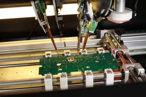
Flying Probe Testing
Flying Probe Testing is similar to ICT but uses a set of movable probes instead of a bed-of-nails fixture. The probes can be programmed to make contact with specific points on the PCB and perform electrical measurements. Flying Probe Testing is more flexible than ICT and can be used to test smaller batches of boards or boards with complex geometries.
Boundary Scan Testing
Boundary Scan Testing, also known as JTAG testing, is a technique used to test the interconnections between components on a PCB. Boundary Scan Testing involves adding special circuitry to the PCB that allows the individual pins of the components to be controlled and observed. This type of testing can detect issues such as:
- Shorts and opens between pins
- Stuck-at faults (pins stuck at a high or low level)
- Incorrect interconnections
Boundary Scan Testing requires that the components on the PCB support the JTAG standard.
Functional Testing
Functional Testing involves testing the PCB as a complete system to ensure that it functions as intended. Functional Testing can be performed using a variety of techniques, such as:
- Manual testing using test equipment
- Automated testing using test software and fixtures
- In-system programming and testing
Functional Testing is typically performed after the PCB has been assembled and tested using other techniques.

Techniques for Testing Electronic Components
There are several techniques that can be used to test electronic components during PCB design:
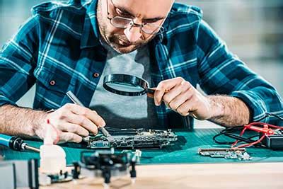
Visual Inspection
Visual Inspection involves examining the PCB and components for any visible defects or issues. This can include checking for:
- Correct component placement and orientation
- Solder joint quality
- Damaged or missing components
- Cleanliness of the PCB
Visual Inspection is typically performed throughout the PCB design and assembly process.
Automated Optical Inspection (AOI)
Automated Optical Inspection (AOI) uses cameras and image processing software to inspect the PCB for defects. AOI can detect issues such as:
- Incorrect component placement or orientation
- Solder joint defects
- Damaged or missing components
- Incorrect labeling or markings
AOI is typically performed after the PCB has been assembled but before it is tested using other techniques.
X-Ray Inspection
X-Ray Inspection uses X-rays to examine the internal structure of the PCB and components. X-Ray Inspection can detect issues such as:
- Voids or cracks in solder joints
- Incorrect component placement or orientation
- Damaged or missing components
- Foreign object debris (FOD)
X-Ray Inspection is typically used for high-reliability applications or for inspecting components that are not visible using other techniques.
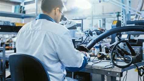
Electrical Testing
Electrical Testing involves measuring the electrical characteristics of the components and interconnections on the PCB. Electrical Testing can be performed using a variety of techniques, such as:
- Continuity testing to check for shorts and opens
- Resistance testing to measure component values
- Capacitance and inductance testing to measure reactive components
- Diode and transistor testing to check for proper function
Electrical Testing is typically performed using specialized test equipment and fixtures.
Best Practices for PCB Testing
To ensure effective PCB testing, there are several best practices that should be followed:
-
Start Testing Early: Testing should be integrated into the PCB design process from the beginning. This allows issues to be identified and fixed early on, reducing the risk of costly redesigns later in the process.
-
Use a Combination of Testing Techniques: No single testing technique can catch all possible issues. Using a combination of techniques, such as ICT, Flying Probe Testing, and Functional Testing, can provide more comprehensive coverage.
-
Develop a Test Plan: A test plan should be developed that outlines the specific tests to be performed, the acceptance criteria, and the resources required. The test plan should be reviewed and approved by all stakeholders.
-
Use Automated Testing Where Possible: Automated testing can improve the speed and accuracy of testing while reducing the risk of human error. Automated testing tools, such as AOI and Flying Probe Testing, should be used where possible.
-
Document Test Results: Test results should be documented and reviewed by the appropriate stakeholders. Any issues identified during testing should be tracked and resolved before moving on to the next phase of the design process.
Common PCB Testing Challenges and Solutions
Despite the many benefits of PCB testing, there are also several challenges that can arise:
Limited Access to Test Points
Some PCBs may have limited access to test points, making it difficult to perform certain types of testing. In these cases, alternative testing techniques, such as Flying Probe Testing or Boundary Scan Testing, may need to be used.
High-Frequency Signals
Testing high-frequency signals can be challenging due to the need for specialized equipment and techniques. High-frequency signals can be affected by factors such as impedance matching, crosstalk, and signal integrity. To test high-frequency signals effectively, designers may need to use techniques such as:
- Time-domain reflectometry (TDR) to measure impedance and detect discontinuities
- Vector network analyzers (VNAs) to measure S-parameters and characterize high-frequency components
- Electromagnetic simulation tools to predict and optimize high-frequency performance
Environmental Factors
Environmental factors, such as temperature, humidity, and vibration, can affect the performance of electronic components and PCBs. To ensure that the PCB will function properly in its intended environment, environmental testing may need to be performed. This can involve subjecting the PCB to various environmental conditions and measuring its performance using techniques such as:
- Temperature cycling to test for thermal expansion and contraction
- Humidity testing to check for moisture resistance
- Vibration testing to ensure mechanical robustness
Cost and Time Constraints
PCB testing can be time-consuming and costly, especially for complex designs or high-volume production. To minimize the impact of testing on the overall design process, designers may need to:
- Prioritize testing based on risk and criticality
- Use design for testability (DFT) techniques to make the PCB easier to test
- Automate testing where possible to reduce time and cost
- Outsource testing to specialized service providers
FAQs
-
What is the difference between ICT and Flying Probe Testing?
ICT uses a bed-of-nails fixture to make contact with specific points on the PCB, while Flying Probe Testing uses movable probes. Flying Probe Testing is more flexible and can be used for smaller batches or complex geometries. -
What is Boundary Scan Testing?
Boundary Scan Testing, also known as JTAG testing, is a technique used to test the interconnections between components on a PCB. It involves adding special circuitry to the PCB that allows individual pins to be controlled and observed. -
What are some common PCB testing challenges?
Common PCB testing challenges include limited access to test points, testing high-frequency signals, environmental factors, and cost and time constraints. -
What are some best practices for PCB testing?
Best practices for PCB testing include starting testing early, using a combination of testing techniques, developing a test plan, using automated testing where possible, and documenting test results. -
Why is PCB testing important?
PCB testing is important for identifying design flaws, ensuring functionality, improving reliability, and reducing manufacturing costs. By catching issues early in the design process, PCB testing can help ensure that the final product meets the required specifications and performs as intended.
Conclusion
PCB testing is a critical aspect of the PCB design process that should not be overlooked. By testing electronic components during the design phase, designers can identify issues early on, reduce the risk of errors, and ensure that the final product meets the required specifications. There are several types of PCB testing, including ICT, Flying Probe Testing, Boundary Scan Testing, and Functional Testing, each with its own advantages and limitations.
To ensure effective PCB testing, designers should follow best practices such as starting testing early, using a combination of testing techniques, developing a test plan, using automated testing where possible, and documenting test results. While PCB testing can present challenges, such as limited access to test points, high-frequency signals, environmental factors, and cost and time constraints, these challenges can be overcome through careful planning and the use of appropriate testing techniques and tools.
In summary, PCB testing is an essential part of the PCB design process that can help ensure the quality, reliability, and performance of the final product. By investing in PCB testing and following best practices, designers can reduce the risk of errors, improve efficiency, and ultimately deliver better products to their customers.
No responses yet