Introduction to PCB Design Challenges
Printed circuit board (PCB) design is a complex process that requires careful planning, attention to detail, and a deep understanding of electronic components and their interactions. One of the most frustrating challenges in PCB design is dealing with unroutable boards – designs that cannot be successfully routed due to various constraints and limitations.
In this article, we will explore practical tips and techniques for overcoming the challenges of unroutable boards in PCB design. By understanding the common causes of unroutability and applying best practices in design, component selection, and layout optimization, you can improve your chances of creating successful, manufacturable PCBs.
Common Causes of Unroutable Boards
Before diving into specific tips, it’s essential to understand the factors that can lead to unroutable boards. Some of the most common causes include:
-
Insufficient board space: When the PCB layout is too small to accommodate all the necessary components and traces, it can result in an unroutable design.
-
High component density: Boards with a large number of components packed tightly together can create routing challenges, especially if there are many interconnections between components.
-
Complex routing requirements: Designs with strict routing constraints, such as high-speed signals, differential pairs, or controlled impedance traces, can be more difficult to route successfully.
-
Inadequate layer stackup: Using too few layers or an inappropriate layer arrangement can limit routing options and lead to unroutable designs.
-
Poor component placement: Inefficient or illogical component placement can create unnecessary routing challenges and contribute to unroutability.

Tips for Avoiding Unroutable Boards
1. Plan Ahead with a Design Review
One of the most effective ways to prevent unroutable boards is to conduct a thorough design review before beginning the PCB layout process. This review should include:
- Schematic analysis: Ensure that the schematic is accurate, complete, and follows best practices for component selection and interconnectivity.
- Bill of Materials (BOM) review: Verify that all components are available, have the correct footprints, and are suitable for the design requirements.
- Mechanical constraints: Consider the physical dimensions of the board, component heights, and any enclosure or mounting requirements.
- Manufacturing capabilities: Consult with your PCB manufacturer to understand their capabilities and limitations, such as minimum trace width and spacing, via sizes, and drill holes.
By identifying potential issues early in the design process, you can make necessary adjustments and avoid unroutable situations later on.
2. Optimize Component Placement
Efficient component placement is crucial for creating routable PCB designs. When placing components, consider the following:
- Grouping: Place related components close together to minimize the length of interconnecting traces.
- Orientation: Orient components in a logical manner that facilitates efficient routing, such as aligning them in rows or columns.
- Spacing: Ensure adequate spacing between components to allow for proper trace routing and clearance.
- Connectors: Position connectors and other external interfaces along the edges of the board for easy access and to avoid blocking internal routing channels.
| Component Type | Placement Guidelines |
|---|---|
| Power Supply | Place near the edge of the board, close to power input |
| High-speed ICs | Group together, minimize trace lengths |
| Decoupling Caps | Place close to IC power pins |
| Connectors | Align along board edges, avoid blocking routing channels |
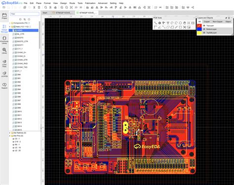
3. Create a Robust Layer Stackup
A well-designed layer stackup can significantly improve the routability of your PCB. Consider the following tips:
- Use an appropriate number of layers: More layers provide additional routing space and flexibility. Consider using 4, 6, or even 8 layers for complex designs.
- Dedicate layers for power and ground: Use separate layers for power and ground planes to improve signal integrity and provide shielding.
- Use inner layers for routing: Route signals on inner layers to free up space on outer layers for components and critical traces.
- Balance copper pour: Ensure a balanced copper distribution across layers to avoid warping and manufacturing issues.
Example 4-layer stackup:
| Layer | Purpose |
|——-|———|
| Top | Components, high-priority traces |
| Inner 1 | Ground plane |
| Inner 2 | Power plane |
| Bottom | Components, general routing |
4. Apply Design for Manufacturing (DFM) Rules
Adhering to DFM rules and guidelines can help ensure that your PCB design is manufacturable and less prone to routing issues. Some key DFM considerations include:
- Trace width and spacing: Use appropriate trace widths and spacing based on the current requirements and PCB manufacturer’s capabilities.
- Via sizes and drill holes: Choose via sizes and drill holes that are compatible with your manufacturer’s equipment and processes.
- Copper pour and clearance: Apply proper copper pour and clearance settings to avoid short circuits and manufacturability problems.
- Solder mask and silkscreen: Ensure adequate solder mask expansion and silkscreen legibility for easy assembly and debugging.
| Parameter | Recommended Value |
|---|---|
| Minimum trace width | 0.15 mm (6 mil) |
| Minimum trace spacing | 0.15 mm (6 mil) |
| Minimum via drill size | 0.3 mm (12 mil) |
| Solder mask expansion | 0.05 mm (2 mil) |
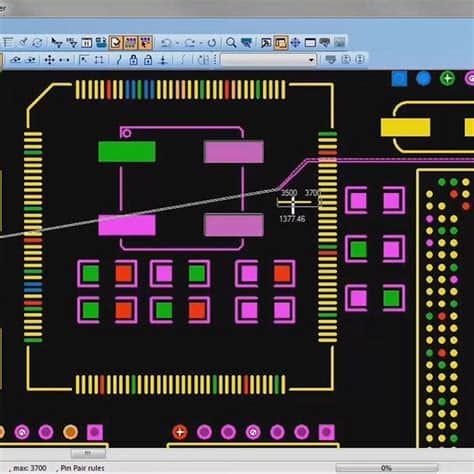
5. Leverage Routing Techniques and Tools
Modern PCB design software offers a range of routing techniques and tools to help overcome unroutable situations. Some valuable techniques include:
- Interactive routing: Manually route critical traces and high-priority signals first, then use auto-routing tools to complete the remaining connections.
- Differential pair routing: Use dedicated tools for routing differential pairs, ensuring proper spacing, and length matching.
- Tuning and optimization: Adjust routing parameters, such as via costs, layer biases, and trace widths, to fine-tune the auto-routing process.
- Design rule checks (DRC): Regularly run DRC to identify and resolve routing violations and potential manufacturability issues.

FAQ
1. What is an unroutable board in PCB design?
An unroutable board is a PCB design that cannot be successfully routed due to various constraints, such as insufficient space, high component density, or complex routing requirements.
2. How can I avoid creating unroutable PCB designs?
To avoid creating unroutable PCB designs, conduct thorough design reviews, optimize component placement, create a robust layer stackup, apply DFM rules, and leverage advanced routing techniques and tools.
3. What is the importance of component placement in PCB routability?
Efficient component placement is crucial for creating routable PCB designs. Grouping related components, orienting them logically, ensuring adequate spacing, and positioning connectors along board edges can significantly improve routability.
4. How does the number of layers affect PCB routability?
Using a higher number of layers, such as 4, 6, or 8, can provide additional routing space and flexibility, making it easier to route complex designs successfully.
5. What are some essential DFM rules to consider for improved routability?
Essential DFM rules for improved routability include using appropriate trace widths and spacing, choosing compatible via sizes and drill holes, applying proper copper pour and clearance settings, and ensuring adequate solder mask expansion and silkscreen legibility.
Conclusion
Designing routable PCBs requires a combination of careful planning, adherence to best practices, and the use of advanced tools and techniques. By understanding the common causes of unroutable boards and applying the tips discussed in this article, you can significantly improve your chances of creating successful, manufacturable PCB designs.
Remember to conduct thorough design reviews, optimize component placement, create robust layer stackups, apply DFM rules, and leverage the power of modern PCB design software. With practice and persistence, you can overcome the challenges of unroutable boards and create PCBs that meet your design requirements and perform reliably in the real world.
No responses yet