
Introduction to Power Delivery Network (PDN) Analysis
In modern electronic systems, the design of the Power Delivery Network (PDN) is crucial for ensuring the reliable operation of the system. PDN analysis is the process of evaluating the performance of the power distribution system in a Printed Circuit Board (PCB) design. The main goal of PDN analysis is to ensure that the power supply can deliver the required current to the various components on the board while maintaining a stable voltage level.
Why is PDN Analysis Important?
PDN analysis is important for several reasons:
- Ensures reliable power delivery to all components on the board
- Minimizes voltage fluctuations and noise
- Prevents signal integrity issues caused by power supply noise
- Helps optimize the placement of decoupling capacitors
- Enables the design of a robust and efficient power distribution system
PDN Design Considerations
When designing a PDN, there are several factors to consider:
Voltage Requirements
The first step in PDN design is to determine the voltage requirements of the various components on the board. This includes the voltage levels, current requirements, and transient response characteristics of each component.
Power Supply Selection
Based on the voltage requirements, the appropriate power supplies must be selected. This includes choosing the right voltage regulators, DC-DC converters, and other power management components.
PDN Topology
The topology of the PDN must be carefully designed to ensure efficient power delivery to all components on the board. This includes the placement of power planes, the use of split planes, and the routing of power traces.
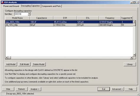
Decoupling Capacitors
Decoupling capacitors are used to provide local energy storage and to filter out high-frequency noise on the power supply lines. The selection and placement of decoupling capacitors is critical for ensuring a stable and clean power supply.
PCB Stackup
The PCB stackup plays a significant role in PDN performance. The number of layers, the thickness of the dielectric material, and the placement of power and ground planes all affect the impedance and current carrying capacity of the PDN.
PDN Analysis Techniques
There are several techniques used for PDN analysis:
DC IR Drop Analysis
DC IR drop analysis is used to determine the voltage drop across the PDN due to the resistance of the conductors. This analysis helps identify areas of the board where the voltage drop may be too high, leading to performance issues.
AC Impedance Analysis
AC impedance analysis is used to evaluate the frequency response of the PDN. This analysis helps identify resonances and other frequency-dependent effects that can cause power supply noise and signal integrity issues.
Transient Analysis
Transient analysis is used to evaluate the response of the PDN to sudden changes in load current. This analysis helps ensure that the power supply can maintain a stable voltage level during transient events such as switching loads or power supply startup.
Thermal Analysis
Thermal analysis is used to evaluate the temperature distribution across the board and to identify hot spots that may affect PDN performance. This analysis helps ensure that the PDN can operate reliably over the expected temperature range.

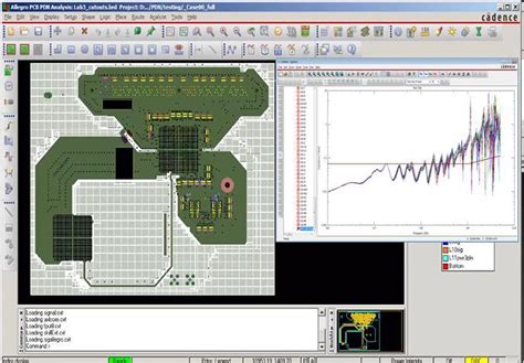
PDN Simulation Tools
There are several software tools available for PDN analysis:
| Tool Name | Vendor | Description |
|---|---|---|
| SIwave | Ansys | 3D full-wave electromagnetic field solver for PDN analysis |
| PDN Analyzer | Cadence | Integrated PDN analysis tool for PCB design |
| HyperLynx PI | Mentor Graphics | Power integrity analysis tool for PCB and package design |
| HFSS | Ansys | 3D full-wave electromagnetic field solver for high-frequency analysis |
These tools provide a range of features for PDN analysis, including:
- DC IR drop analysis
- AC impedance analysis
- Transient analysis
- Decoupling capacitor optimization
- PCB stackup analysis
- Thermal analysis
Best Practices for PDN Design
Here are some best practices for designing a robust and efficient PDN:
- Use a solid ground plane to provide a low-impedance return path for current.
- Place decoupling capacitors close to the power pins of ICs to minimize the loop inductance.
- Use multiple layers for power and ground to reduce inductance and resistance.
- Minimize the use of vias in the power and ground planes to reduce inductance.
- Use wide traces for high-current paths to minimize resistance and voltage drop.
- Optimize the placement and values of decoupling capacitors using simulation tools.
- Consider the use of embedded capacitance materials in the PCB stackup to reduce the number of discrete capacitors needed.
- Use separate power planes for analog and digital circuitry to minimize noise coupling.
- Perform thorough PDN analysis early in the design process to identify and correct issues before fabrication.
- Work closely with the PCB fabricator to ensure that the stackup and materials are optimized for PDN performance.
Conclusion
PDN analysis is a critical aspect of PCB design that ensures the reliable and efficient operation of electronic systems. By considering factors such as voltage requirements, power supply selection, PDN topology, decoupling capacitors, and PCB stackup, designers can create a robust and optimized PDN. The use of simulation tools and best design practices can help identify and correct issues early in the design process, reducing the risk of costly redesigns and improving overall system performance.
Frequently Asked Questions (FAQ)
- What is PDN analysis?
-
PDN analysis is the process of evaluating the performance of the power distribution network in a PCB design to ensure reliable and efficient power delivery to all components on the board.
-
Why is PDN analysis important?
-
PDN analysis is important because it helps ensure reliable power delivery, minimizes voltage fluctuations and noise, prevents signal integrity issues, optimizes decoupling capacitor placement, and enables the design of a robust and efficient power distribution system.
-
What factors should be considered when designing a PDN?
-
When designing a PDN, factors to consider include voltage requirements, power supply selection, PDN topology, decoupling capacitors, and PCB stackup.
-
What are some common PDN analysis techniques?
-
Common PDN analysis techniques include DC IR drop analysis, AC impedance analysis, transient analysis, and thermal analysis.
-
What are some best practices for PDN design?
- Some best practices for PDN design include using solid ground planes, placing decoupling capacitors close to IC power pins, using multiple layers for power and ground, minimizing via usage in power and ground planes, using wide traces for high-current paths, optimizing decoupling capacitor placement and values, considering embedded capacitance materials, using separate power planes for analog and digital circuitry, performing thorough PDN analysis early in the design process, and working closely with the PCB fabricator to optimize stackup and materials.
No responses yet