Introduction to PTH Vias in mmWave PCB Design
Plated through hole (PTH) vias are an essential component in the design and fabrication of printed circuit boards (PCBs) for millimeter-wave (mmWave) applications. As the demand for high-frequency, high-speed communication systems continues to grow, the importance of optimizing PCB design for mmWave frequencies becomes increasingly critical. PTH vias play a crucial role in interconnecting different layers of a multi-layer PCB, enabling the transmission of high-frequency signals while maintaining signal integrity.
In this article, we will delve into the world of PTH vias in mmWave PCB design, exploring their significance, design considerations, fabrication techniques, and best practices for optimizing performance. We will also address common challenges and provide insights into the future trends of PTH via technology in mmWave applications.
The Significance of PTH Vias in mmWave PCBs
Signal Integrity and Transmission
PTH vias are fundamental to maintaining signal integrity in mmWave PCBs. At high frequencies, signal loss, reflections, and crosstalk become significant concerns. PTH vias provide a low-impedance path for signals to traverse between layers, minimizing signal degradation and ensuring reliable transmission. By carefully designing the via geometry, spacing, and placement, engineers can optimize signal integrity and minimize losses in mmWave PCBs.
Thermal Management
In addition to their role in signal transmission, PTH vias also contribute to the thermal management of mmWave PCBs. High-frequency circuits generate significant amounts of heat, which can adversely affect performance and reliability. PTH vias act as thermal conduits, allowing heat to dissipate from hot spots on the PCB to other layers or external heat sinks. By strategically placing PTH vias near heat-generating components, designers can improve the overall thermal performance of the PCB.
Mechanical Strength and Reliability
PTH vias also provide mechanical strength and reliability to mmWave PCBs. The plated holes create a strong mechanical connection between layers, enhancing the overall structural integrity of the board. This is particularly important in applications where the PCB is subjected to mechanical stress, vibrations, or thermal cycling. PTH vias help prevent delamination and improve the long-term reliability of mmWave PCBs.
Design Considerations for PTH Vias in mmWave PCBs
Via Geometry and Dimensions
The geometry and dimensions of PTH vias play a critical role in their performance at mmWave frequencies. The diameter of the via hole, the thickness of the plating, and the pad size all influence the electrical characteristics of the via. Smaller via diameters are generally preferred for mmWave applications to minimize capacitance and inductance. However, the via dimensions must also consider manufacturability and reliability constraints.
| Parameter | Typical Value |
|---|---|
| Via Hole Diameter | 0.1 mm – 0.3 mm |
| Plating Thickness | 25 μm – 50 μm |
| Pad Diameter | 0.2 mm – 0.5 mm |
Via Placement and Spacing
The placement and spacing of PTH vias in mmWave PCBs are crucial for optimizing signal integrity and minimizing interference. Vias should be placed as close as possible to the signal source or destination to reduce the via stub length. Via stubs act as resonant structures that can cause signal reflections and losses at mmWave frequencies. By minimizing the stub length, designers can mitigate these undesirable effects.
Additionally, the spacing between vias should be carefully considered to prevent crosstalk and coupling between adjacent signals. Adequate via-to-via spacing helps maintain signal isolation and reduces the risk of interference.
| Parameter | Typical Value |
|---|---|
| Via Stub Length | < 0.1 mm |
| Via-to-Via Spacing | > 2 × Via Diameter |
Ground Vias and Shielding
Ground vias play a vital role in providing a low-impedance return path for high-frequency signals and shielding against electromagnetic interference (EMI). In mmWave PCBs, ground vias are strategically placed near signal vias to create a controlled impedance environment and minimize radiation. By surrounding signal vias with ground vias, designers can create a coaxial-like structure that confines the electromagnetic fields and reduces crosstalk.
The number and placement of ground vias depend on the signal frequency, PCB stackup, and routing requirements. Simulation tools and electromagnetic modeling can help optimize the ground via configuration for optimal shielding and signal integrity.

Fabrication Techniques for PTH Vias in mmWave PCBs
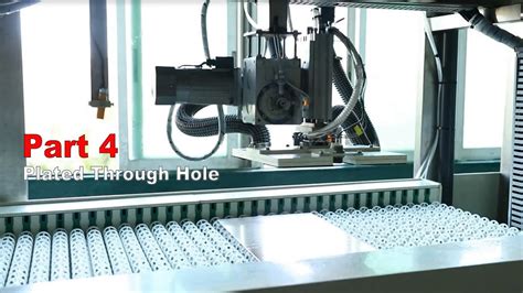
Drilling and Plating
The fabrication of PTH vias in mmWave PCBs involves precise drilling and plating processes. High-speed, high-precision drilling machines are used to create the via holes in the PCB substrate. The drilling process must ensure accurate hole placement, minimal deviation from the specified diameter, and smooth hole walls to facilitate reliable plating.
After drilling, the via holes are plated with a conductive material, typically copper, to create an electrical connection between layers. The plating process involves several steps, including cleaning, activation, electroless copper deposition, and electroplating. The plating thickness and uniformity are critical for achieving the desired electrical performance and reliability.
Filling and Capping
In some cases, PTH vias in mmWave PCBs are filled or capped to improve signal integrity and mechanical stability. Via filling involves depositing a conductive or non-conductive material into the via hole to eliminate the air gap and create a solid connection. Conductive filling materials, such as copper or silver epoxy, provide electrical continuity and help dissipate heat. Non-conductive filling materials, such as epoxy or resin, improve mechanical strength and prevent moisture ingress.
Via capping is another technique used to enhance the performance of PTH vias. In this process, a conductive cap is applied over the via pad on one or both sides of the PCB. Via capping helps reduce the via stub effect, improves signal reflection, and provides better shielding against EMI.
Best Practices for Optimizing PTH Via Performance
Simulation and Modeling
To optimize the performance of PTH vias in mmWave PCBs, designers rely on simulation and modeling tools. Electromagnetic simulation software, such as HFSS or CST, allows engineers to analyze the electrical behavior of vias at high frequencies. These tools help identify potential signal integrity issues, optimize via geometry and placement, and evaluate the impact of different design parameters.
Modeling techniques, such as finite element analysis (FEA) and computational fluid dynamics (CFD), are also used to study the thermal and mechanical behavior of PTH vias. These simulations help ensure that the vias can effectively dissipate heat and withstand mechanical stresses during assembly and operation.
Material Selection
The choice of materials for PTH vias in mmWave PCBs is critical for achieving optimal performance. The substrate material, plating metal, and filling or capping materials all influence the electrical, thermal, and mechanical properties of the vias.
Low-loss, high-frequency substrates, such as Rogers or Taconic materials, are commonly used for mmWave PCBs. These materials offer excellent dielectric properties, low dissipation factors, and controlled thermal expansion. The plating metal, typically copper, should have high conductivity, good adhesion to the substrate, and compatibility with the selected finishing process.
Filling and capping materials should be chosen based on their electrical and thermal conductivity, adhesion strength, and ease of processing. Conductive materials like copper or silver epoxy provide the best electrical performance, while non-conductive materials offer improved mechanical stability.
Testing and Validation
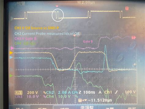
Rigorous testing and validation are essential to ensure the reliability and performance of PTH vias in mmWave PCBs. Electrical testing, such as time-domain reflectometry (TDR) and vector network analyzer (VNA) measurements, helps characterize the impedance, insertion loss, and return loss of the vias. These measurements provide valuable insights into the signal integrity and help identify any discontinuities or reflections.
Thermal testing, using techniques like infrared thermography or thermocouples, helps evaluate the thermal performance of PTH vias. By measuring the temperature distribution across the PCB and identifying hot spots, designers can optimize the via placement and sizing for effective heat dissipation.
Mechanical testing, including cross-sectioning and microsectioning, allows designers to inspect the quality of the via plating, filling, and capping. These tests help identify any voids, cracks, or delamination that could compromise the reliability of the vias.
Future Trends in PTH Via Technology for mmWave PCBs
As the demand for higher data rates and increased bandwidth continues to drive the development of mmWave systems, PTH via technology is evolving to meet the challenges. Some of the future trends in PTH via technology for mmWave PCBs include:
-
Advanced materials: The development of new substrate materials with improved dielectric properties, lower loss tangents, and better thermal stability will enable the design of high-performance PTH vias for mmWave applications.
-
3D printing: The adoption of 3D printing technologies, such as selective laser sintering (SLS) or stereolithography (SLA), for PCB fabrication will allow for greater design flexibility and the creation of complex via structures.
-
Embedded vias: The integration of embedded vias, where the vias are formed within the PCB substrate rather than drilled through, will offer improved signal integrity, reduced via stub effects, and higher component density.
-
Active vias: The incorporation of active components, such as transistors or diodes, directly into the via structure will enable advanced functionalities like signal amplification or switching within the PCB.
-
Optical vias: The exploration of optical via technology, using photonic materials and optical interconnects, will pave the way for high-speed, low-loss signal transmission in mmWave PCBs.
FAQ
Q1: What is the main purpose of PTH vias in mmWave PCBs?
A1: The main purpose of PTH vias in mmWave PCBs is to provide electrical connections between different layers of the PCB while maintaining signal integrity and minimizing losses at high frequencies.
Q2: What are the key design considerations for PTH vias in mmWave PCBs?
A2: The key design considerations for PTH vias in mmWave PCBs include via geometry and dimensions, via placement and spacing, ground via configuration, and material selection. These factors influence the electrical, thermal, and mechanical performance of the vias.
Q3: How can simulation and modeling tools help optimize PTH via performance?
A3: Simulation and modeling tools, such as electromagnetic simulation software and finite element analysis, help designers analyze the electrical, thermal, and mechanical behavior of PTH vias. These tools enable the optimization of via geometry, placement, and materials for improved signal integrity and reliability.
Q4: What are some common fabrication techniques for PTH vias in mmWave PCBs?
A4: Common fabrication techniques for PTH vias in mmWave PCBs include high-precision drilling, plating, filling, and capping. These processes ensure accurate via formation, reliable electrical connections, and enhanced mechanical stability.
Q5: What are some future trends in PTH via technology for mmWave PCBs?
A5: Future trends in PTH via technology for mmWave PCBs include the development of advanced materials, the adoption of 3D printing for PCB fabrication, the integration of embedded vias, the incorporation of active components into via structures, and the exploration of optical via technology.
Conclusion
Plated through hole (PTH) vias are a critical component in the design and fabrication of mmWave PCBs. They provide reliable electrical connections between layers, maintain signal integrity, and contribute to thermal management and mechanical stability. By carefully considering via geometry, placement, spacing, and material selection, designers can optimize the performance of PTH vias for high-frequency applications.
As mmWave technology continues to advance, PTH via technology will evolve to meet the increasing demands for higher data rates, improved signal integrity, and greater reliability. The adoption of advanced materials, innovative fabrication techniques, and emerging technologies like active and optical vias will shape the future of PTH vias in mmWave PCBs.
By staying up-to-date with the latest trends and best practices in PTH via design and fabrication, engineers can unlock the full potential of mmWave systems and drive the development of next-generation wireless communications.
No responses yet