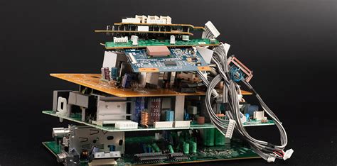
Introduction to PCB and Electronics Failures
Printed Circuit Boards (PCBs) and electronic assemblies are critical components in modern technology, powering devices ranging from smartphones to aerospace systems. However, these intricate systems are susceptible to various failure mechanisms, often stemming from the physical stresses and environmental factors they encounter during operation. Understanding the physics behind these failures is crucial for designing robust and reliable electronics.
In this article, we will delve into the world of PCB and electronics failures, exploring the common causes, mechanisms, and mitigation strategies. We will also discuss the importance of failure analysis and reliability testing in ensuring the longevity and performance of electronic systems.
Common Causes of PCB and Electronics Failures
Thermal Stress
Thermal stress is one of the most prevalent causes of PCB and electronics failures. Temperature fluctuations, whether due to environmental conditions or the heat generated by the components themselves, can lead to a range of issues:
-
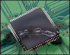
Thermal Expansion and Contraction: As temperature changes, materials expand or contract at different rates, causing mechanical stress on the PCB and its components. This can lead to cracking, delamination, and warping of the board.
-
Solder Joint Fatigue: Repeated thermal cycling can cause solder joints to weaken and eventually fail, leading to intermittent connections or complete loss of functionality.
-
Component Degradation: Prolonged exposure to high temperatures can cause components to degrade, affecting their performance and reliability.
Mechanical Stress
PCBs and electronic assemblies are also susceptible to mechanical stresses, which can arise from various sources:
-
Vibration and Shock: Exposure to vibration and shock, especially in automotive and aerospace applications, can cause components to become loose or damaged, leading to failures.
-
Flexing and Bending: Excessive flexing or bending of the PCB can cause trace cracking, component damage, and solder joint failures.
-
Physical Impact: Accidental drops or impacts can cause severe damage to PCBs and their components, often resulting in immediate failure.
Chemical and Environmental Factors
The environment in which PCBs and electronics operate can also contribute to failures:
-
Corrosion: Exposure to moisture, pollutants, and corrosive agents can lead to the degradation of PCB materials and components, causing short circuits and other malfunctions.
-
Electrostatic Discharge (ESD): ESD events can damage sensitive components, particularly in the absence of proper ESD protection measures.
-
Electromagnetic Interference (EMI): External EMI sources can disrupt the operation of electronic systems, causing data corruption or system failures.
Failure Mechanisms and Analysis Techniques
To effectively mitigate PCB and electronics failures, it is essential to understand the underlying mechanisms and employ appropriate analysis techniques.
Failure Mechanisms
-
Fatigue: Repeated stress cycles can lead to the gradual accumulation of damage, ultimately resulting in failure. Fatigue can affect solder joints, component leads, and PCB traces.
-
Creep: Prolonged exposure to high temperatures and mechanical stress can cause materials to deform slowly over time, leading to failures such as component misalignment or solder joint fractures.
-
Electromigration: High current densities can cause metal ions to migrate, leading to the formation of voids and hillocks in conductors, eventually causing open or short circuits.
Failure Analysis Techniques
-
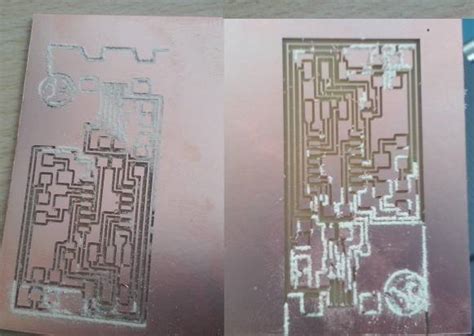
Visual Inspection: A thorough visual examination of the PCB and components can reveal signs of physical damage, corrosion, or manufacturing defects.
-
X-Ray Imaging: X-ray techniques allow for non-destructive inspection of solder joints, component placement, and internal structures.
-
Microsectioning: Cross-sectioning of the PCB and components enables detailed analysis of internal structures, helping to identify failures such as delamination or cracking.
-
Scanning Electron Microscopy (SEM): SEM provides high-resolution imaging of surface features, allowing for the identification of micro-cracks, corrosion, and other small-scale defects.
-
Electrical Testing: Functional and in-circuit testing can help pinpoint malfunctioning components or circuits, aiding in the identification of failure locations.

Reliability Testing and Mitigation Strategies
To ensure the reliability and longevity of PCBs and electronic assemblies, it is crucial to employ appropriate testing methods and implement effective mitigation strategies.
Reliability Testing
-
Accelerated Life Testing (ALT): ALT subjects the PCB or assembly to elevated stress levels (e.g., temperature, humidity, vibration) to accelerate the occurrence of failures, allowing for the estimation of product lifetime under normal operating conditions.
-
Thermal Cycling: Exposing the PCB to repeated temperature cycles helps identify weaknesses in solder joints and other temperature-sensitive components.
-
Vibration and Shock Testing: Subjecting the PCB to controlled vibration and shock loads helps assess its ability to withstand mechanical stresses encountered in the intended application.
-
Humidity Testing: Exposing the PCB to high humidity levels can reveal susceptibility to corrosion and moisture-related failures.
Mitigation Strategies
-
Design for Reliability (DfR): Incorporating DfR principles during the design phase, such as selecting appropriate materials, optimizing component placement, and implementing redundancy, can significantly enhance the reliability of PCBs and electronics.
-
Thermal Management: Effective thermal management techniques, such as using heat sinks, thermal interface materials, and proper ventilation, can help dissipate heat and reduce thermal stress on components.
-
Conformal Coating: Applying a conformal coating to the PCB can provide protection against moisture, contaminants, and corrosion.
-
Strain Relief: Incorporating strain relief features, such as flexible interconnects or stress-reducing mounting methods, can minimize the impact of mechanical stresses on the PCB and components.
-
Quality Control and Inspection: Implementing robust quality control measures, including incoming material inspection, process control, and post-assembly testing, can help identify and eliminate defects before they lead to failures in the field.
Case Studies
Case Study 1: Solder Joint Failure in Automotive Electronics
In an automotive application, a PCB controlling the engine management system experienced intermittent malfunctions. Failure analysis revealed that the root cause was solder joint fatigue caused by repeated thermal cycling. The solution involved redesigning the PCB layout to minimize thermal stress on the affected joints and implementing a more robust solder alloy.
Case Study 2: Corrosion-Induced Failure in Industrial Sensors
An industrial sensor deployed in a harsh environment experienced sudden failures. Investigation showed that corrosion of the PCB and components due to exposure to corrosive gases was the primary cause. The issue was addressed by applying a conformal coating to the PCB and selecting components with better corrosion resistance.
Frequently Asked Questions (FAQ)
-
Q: What are the most common causes of PCB and electronics failures?
A: The most common causes include thermal stress, mechanical stress, and chemical/environmental factors such as corrosion, ESD, and EMI. -
Q: How can thermal stress lead to PCB failures?
A: Thermal stress can cause issues such as thermal expansion and contraction, solder joint fatigue, and component degradation, leading to cracking, delamination, and loss of functionality. -
Q: What is the importance of failure analysis in PCB and electronics reliability?
A: Failure analysis helps identify the root causes of failures, enabling engineers to develop targeted mitigation strategies and improve the overall reliability of the system. -
Q: How can reliability testing help prevent PCB and electronics failures?
A: Reliability testing, such as accelerated life testing and thermal cycling, subjects the PCB to elevated stress levels, helping identify weaknesses and potential failure modes before the product is deployed in the field. -
Q: What are some effective mitigation strategies for preventing PCB and electronics failures?
A: Effective mitigation strategies include Design for Reliability (DfR), thermal management, conformal coating, strain relief, and robust quality control measures.
Conclusion
PCB and electronics failures can have significant consequences, ranging from minor inconveniences to catastrophic system failures. By understanding the physics behind these failures, employing appropriate analysis techniques, and implementing effective mitigation strategies, engineers can design more reliable and robust electronic systems.
Investing in failure analysis and reliability testing is crucial for identifying potential issues early in the development process, allowing for timely corrective actions and ultimately reducing the risk of failures in the field. As technology continues to advance, the importance of addressing PCB and electronics failures will only continue to grow, making it imperative for engineers to stay informed and proactive in ensuring the reliability of these critical components.
No responses yet