Introduction to PCB Shielding
In the world of electronic design, ensuring the integrity and reliability of printed circuit boards (PCBs) is of utmost importance. One critical aspect of PCB design is shielding, which plays a vital role in protecting the circuit from electromagnetic interference (EMI), radio frequency interference (RFI), and other external disturbances. This comprehensive article will delve into the intricacies of PCB shielding, exploring its benefits, techniques, and best practices to help you fortify your designs like a phalanx and avoid failure.
Understanding Electromagnetic Interference (EMI) and Radio Frequency Interference (RFI)
Before we dive into PCB shielding, it’s essential to grasp the concepts of EMI and RFI. EMI refers to the disruption of an electronic device’s operation due to electromagnetic waves emitted by other devices or sources. RFI, on the other hand, specifically pertains to interference caused by radio frequency signals. Both EMI and RFI can lead to signal degradation, data corruption, and even complete system failure if left unchecked.
Sources of EMI and RFI
EMI and RFI can originate from various sources, both internal and external to the PCB. Some common sources include:
- Power supplies and voltage regulators
- High-speed digital circuits
- Wireless communication devices (e.g., Wi-Fi, Bluetooth)
- Electrostatic discharge (ESD)
- Nearby electronic devices and appliances
Effects of EMI and RFI on PCBs
The detrimental effects of EMI and RFI on PCBs can manifest in several ways:
- Signal integrity issues
- Crosstalk between adjacent traces
- Increased noise levels
- Reduced signal-to-noise ratio (SNR)
- Intermittent or complete system failure
PCB Shielding Techniques
To combat the threats posed by EMI and RFI, designers employ various PCB shielding techniques. These techniques aim to create a protective barrier around sensitive components and traces, effectively blocking or attenuating unwanted electromagnetic waves. Let’s explore some of the most common PCB shielding techniques.
Ground Planes and Traces
One of the most fundamental PCB shielding techniques is the use of ground planes and traces. By strategically placing ground planes and traces around sensitive components and signal traces, designers can create a low-impedance return path for high-frequency currents. This helps to minimize the loop area and reduce the radiation of electromagnetic waves.
Benefits of Ground Planes and Traces
- Reduces EMI and RFI emissions
- Improves signal integrity
- Provides a stable reference voltage
- Enhances heat dissipation
Design Considerations for Ground Planes and Traces
- Ensure proper grounding of components
- Minimize the distance between signal traces and ground planes
- Use a solid ground plane instead of a mesh or hatched pattern
- Avoid discontinuities in the ground plane
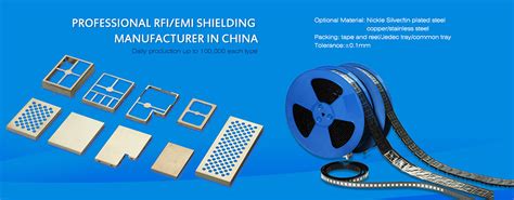
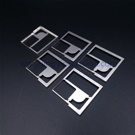
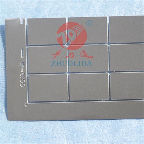
Shielding Enclosures and Cans
Another effective PCB shielding technique is the use of shielding enclosures and cans. These are metallic structures that surround sensitive components or entire sections of the PCB, creating a Faraday cage that blocks external electromagnetic waves. Shielding enclosures and cans come in various shapes and sizes, depending on the specific requirements of the design.
Types of Shielding Enclosures and Cans
- Stamped metal cans
- Drawn metal cans
- Conductive plastic enclosures
- Board-level shielding (BLS) cans
Factors to Consider When Selecting Shielding Enclosures and Cans
- Material properties (conductivity, permeability)
- Mechanical strength and durability
- Ease of assembly and disassembly
- Cost and availability
EMI/RFI Filters and Suppression Components
In addition to shielding enclosures and ground planes, designers can also employ EMI/RFI filters and suppression components to mitigate the effects of electromagnetic interference. These components work by attenuating or filtering out unwanted frequencies while allowing desired signals to pass through unimpeded.
Common EMI/RFI Filters and Suppression Components
- Capacitors (ceramic, tantalum, electrolytic)
- Inductors and ferrite beads
- Common mode chokes
- Transient voltage suppressors (TVS)
- Shielded cables and connectors
Selecting the Right EMI/RFI Filters and Suppression Components
When choosing EMI/RFI filters and suppression components, consider the following factors:
- Frequency range of operation
- Current and voltage ratings
- Insertion loss and attenuation characteristics
- Package size and mounting options
- Environmental conditions (temperature, humidity)

PCB Layout Techniques for Improved Shielding
Effective PCB shielding goes beyond the use of specific components and enclosures. The layout of the PCB itself plays a crucial role in minimizing EMI and RFI. By following best practices in PCB layout, designers can significantly reduce the susceptibility of their designs to electromagnetic interference.
Component Placement and Routing
Proper component placement and routing are essential for effective PCB shielding. Here are some guidelines to follow:
- Group components based on their function and frequency of operation
- Minimize the distance between components and their associated ground planes
- Route high-speed signals away from sensitive analog components
- Use short and direct traces to reduce loop areas and minimize radiation
Layering and Stackup
The layering and stackup of a PCB can also impact its shielding performance. Consider the following tips:
- Use multiple ground planes to provide shielding between layers
- Alternate signal and ground layers to minimize crosstalk
- Use a symmetrical stackup to balance the electromagnetic fields
- Ensure proper via spacing and placement to maintain shielding continuity
Grounding and Power Distribution
Effective grounding and power distribution are critical for PCB shielding. Follow these best practices:
- Use a star grounding topology to minimize ground loops
- Separate analog and digital ground planes to reduce noise coupling
- Implement proper decoupling and bypass capacitors near power pins
- Use a power plane instead of traces for low-impedance power distribution
Testing and Validation of PCB Shielding
Once the PCB design is complete, it’s crucial to test and validate its shielding performance to ensure it meets the required standards and specifications. Several methods can be employed to assess the effectiveness of PCB shielding.
EMC Testing
Electromagnetic compatibility (EMC) testing is a comprehensive approach to evaluating the shielding performance of a PCB. EMC testing involves subjecting the PCB to various electromagnetic disturbances and measuring its response. Common EMC tests include:
- Radiated emissions testing
- Conducted emissions testing
- Radiated susceptibility testing
- Conducted susceptibility testing
Near-Field Scanning
Near-field scanning is a technique used to identify localized sources of EMI and RFI on a PCB. By using a near-field probe, designers can map the electromagnetic field distribution over the surface of the PCB and pinpoint areas that require additional shielding or layout modifications.
Thermal Imaging
Thermal imaging can be used to detect hot spots on a PCB that may indicate the presence of high-frequency currents or EMI-induced heating. By identifying these areas, designers can make targeted improvements to the shielding design to mitigate the effects of electromagnetic interference.
Case Studies and Real-World Examples
To illustrate the importance and effectiveness of PCB shielding, let’s examine some real-world case studies and examples.
Case Study 1: Automotive Electronic Control Unit (ECU)
In the automotive industry, electronic control units (ECUs) are responsible for managing various vehicle functions, from engine control to infotainment systems. Given the harsh electromagnetic environment in which these ECUs operate, effective PCB shielding is paramount.
One automotive manufacturer faced issues with EMI-induced failures in their ECUs, leading to costly recalls and customer dissatisfaction. By implementing a combination of shielding techniques, including the use of shielding cans, ground planes, and EMI filters, the manufacturer was able to significantly reduce the occurrence of EMI-related failures and improve the overall reliability of their ECUs.
Case Study 2: Medical Device Shielding
Medical devices, such as patient monitors and imaging equipment, are subject to stringent EMC regulations to ensure patient safety and device performance. In one case, a medical device manufacturer encountered challenges in meeting the required EMC standards for their new patient monitor.
By collaborating with a PCB shielding expert, the manufacturer was able to redesign the PCB layout, incorporate shielding enclosures, and optimize the grounding and power distribution. These modifications allowed the patient monitor to pass the necessary EMC tests and obtain regulatory approval, enabling the manufacturer to bring their product to market successfully.
Frequently Asked Questions (FAQ)
- What is the difference between EMI and RFI?
-
EMI (electromagnetic interference) refers to the broader category of interference caused by electromagnetic waves, while RFI (radio frequency interference) specifically pertains to interference caused by radio frequency signals.
-
How do I choose the right shielding enclosure for my PCB?
-
When selecting a shielding enclosure, consider factors such as material properties, mechanical strength, ease of assembly, and cost. Consult with shielding experts or suppliers to determine the best option for your specific application.
-
Can PCB shielding completely eliminate EMI and RFI?
-
While PCB shielding can significantly reduce the effects of EMI and RFI, it is challenging to completely eliminate them. The goal is to attenuate the interference to a level that does not compromise the functionality or performance of the PCB.
-
What role does PCB layout play in shielding effectiveness?
-
PCB layout is crucial for effective shielding. Proper component placement, routing, layering, and grounding techniques can help minimize the susceptibility of the PCB to EMI and RFI, enhancing overall shielding performance.
-
How do I test the shielding effectiveness of my PCB?
- Various methods can be used to test PCB shielding effectiveness, including EMC testing, near-field scanning, and thermal imaging. Consult with EMC testing labs or experts to determine the most appropriate testing approach for your specific PCB design.
Conclusion
PCB shielding is a critical aspect of electronic design that ensures the integrity, reliability, and performance of printed circuit boards in the face of electromagnetic interference. By understanding the sources and effects of EMI and RFI, and employing a combination of shielding techniques, such as ground planes, shielding enclosures, and EMI/RFI filters, designers can create a robust phalanx to protect their PCBs from failure.
Moreover, by following best practices in PCB layout, including component placement, routing, layering, and grounding, designers can further enhance the effectiveness of their shielding solutions. Testing and validation, through methods like EMC testing and near-field scanning, are essential to ensure that the PCB meets the required standards and specifications.
As demonstrated by the real-world case studies, effective PCB shielding can mean the difference between a successful product launch and costly failures. By prioritizing PCB shielding in the design process and collaborating with shielding experts, manufacturers can deliver reliable, high-performance electronic devices that stand the test of time.
In conclusion, PCB shielding is not an option but a necessity in today’s increasingly complex and interconnected electronic landscape. By fortifying your PCB designs with the right shielding techniques and best practices, you can create a phalanx that will protect your devices from the perils of electromagnetic interference, ensuring their success in the marketplace.
No responses yet